Refine search
Actions for selected content:
106102 results in Materials Science
4 - Energy cost of materials: materials for thin-film photovoltaics as an example
- from Part 1 - Energy and the environment: the global landscape
-
-
- Book:
- Fundamentals of Materials for Energy and Environmental Sustainability
- Published online:
- 05 June 2012
- Print publication:
- 30 November 2011, pp 48-60
-
- Chapter
- Export citation
21 - Concentrating solar thermal power
- from Part 3 - Renewable energy sources
-
-
- Book:
- Fundamentals of Materials for Energy and Environmental Sustainability
- Published online:
- 05 June 2012
- Print publication:
- 30 November 2011, pp 272-288
-
- Chapter
- Export citation
42 - Toward the smart grid: the US as a case study
- from Part 6 - Energy storage, high-penetration renewables, and grid stabilization
-
-
- Book:
- Fundamentals of Materials for Energy and Environmental Sustainability
- Published online:
- 05 June 2012
- Print publication:
- 30 November 2011, pp 578-593
-
- Chapter
- Export citation

Diffusion characteristics study of locally Er-doped noncongruent, Li-deficient Ti:Er:LiNbO3 strip waveguide
-
- Journal:
- Journal of Materials Research / Volume 26 / Issue 23 / 14 December 2011
- Published online by Cambridge University Press:
- 25 November 2011, pp. 2924-2930
- Print publication:
- 14 December 2011
-
- Article
- Export citation

The Snomipede: A parallel platform for scanning near-field photolithography
-
- Journal:
- Journal of Materials Research / Volume 26 / Issue 24 / 28 December 2011
- Published online by Cambridge University Press:
- 25 November 2011, pp. 2997-3008
- Print publication:
- 28 December 2011
-
- Article
- Export citation
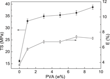
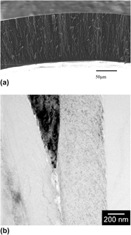
Oxidized starch films reinforced with natural halloysite
-
- Journal:
- Journal of Materials Research / Volume 26 / Issue 23 / 14 December 2011
- Published online by Cambridge University Press:
- 25 November 2011, pp. 2938-2944
- Print publication:
- 14 December 2011
-
- Article
- Export citation

Effects of resin type on properties of graphite/polymer composite bipolar plate for proton exchange membrane fuel cell
-
- Journal:
- Journal of Materials Research / Volume 26 / Issue 23 / 14 December 2011
- Published online by Cambridge University Press:
- 25 November 2011, pp. 2974-2979
- Print publication:
- 14 December 2011
-
- Article
- Export citation
Thick beryllium coatings by ion-assisted magnetron sputtering
-
- Journal:
- Journal of Materials Research / Volume 27 / Issue 5 / 14 March 2012
- Published online by Cambridge University Press:
- 24 November 2011, pp. 822-828
- Print publication:
- 14 March 2012
-
- Article
- Export citation

Microscale deformation of (001) and (100) rutile single crystals under spherical nanoindentation
-
- Journal:
- Journal of Materials Research / Volume 27 / Issue 1 / 14 January 2012
- Published online by Cambridge University Press:
- 24 November 2011, pp. 53-63
- Print publication:
- 14 January 2012
-
- Article
- Export citation
-
Herein rutile (TiO2) single-crystal surfaces, with (001) and (100) orientations, were indented with hemispherical indenters with radii of 13.5, 5, and 1.4 μm. By converting the load–displacement data to nanoindentation (NI) stress–strain curves, together with microscopic post-indentation observations, we conclude that in the (001) orientation, plastic deformation occurs by the activation of all four {101}<10
 > slip systems. In the (100) orientation, only two of the four {101}<10
 > slip systems, along with {100}<0
 0> slip, are activated. Because the four {101}<10
 > slip systems in the (001) orientation intersect, the surface is harder and exhibits higher hardening rates after the nucleation of dislocations. The latter are manifested by pop-ins, some of which are large. The pop-in stresses are adequately described by Weibull statistics and were significantly higher for the (001) orientation. The elastic moduli, determined from spherical NI stiffness versus contact radii plots, were 349 ± 5 and 229 ± 4 GPa for (001) and (100) orientations, respectively. Fully spontaneous reversible, stress–strain hysteretic curves—only manifest in the (100) orientation—are attributed to the to-and-fro motion of dislocations comprising incipient kink bands in the {100}<0
 0> slip system.
Use of spherical indentation technique for measurement of property variations of γTiAl
-
- Journal:
- Journal of Materials Research / Volume 27 / Issue 1 / 14 January 2012
- Published online by Cambridge University Press:
- 24 November 2011, pp. 378-388
- Print publication:
- 14 January 2012
-
- Article
- Export citation

Structural characterization of B-doped diamond nanoindentation tips
-
- Journal:
- Journal of Materials Research / Volume 26 / Issue 24 / 28 December 2011
- Published online by Cambridge University Press:
- 24 November 2011, pp. 3051-3057
- Print publication:
- 28 December 2011
-
- Article
- Export citation

Structure-property-performance of nanocomposite Cr–Si–N films synthesized by a duplex surface treatment technique
-
- Journal:
- Journal of Materials Research / Volume 26 / Issue 24 / 28 December 2011
- Published online by Cambridge University Press:
- 24 November 2011, pp. 3020-3031
- Print publication:
- 28 December 2011
-
- Article
- Export citation

Distribution of visible luminescence centers in hydrogen-doped ZnO
-
- Journal:
- Journal of Materials Research / Volume 26 / Issue 23 / 14 December 2011
- Published online by Cambridge University Press:
- 23 November 2011, pp. 2912-2915
- Print publication:
- 14 December 2011
-
- Article
- Export citation

A critical evaluation of reactive templated grain growth (RTGG) mechanisms in highly [001] textured Sr0.61Ba0.39Nb2O6 ferroelectric-thermoelectrics
-
- Journal:
- Journal of Materials Research / Volume 26 / Issue 24 / 28 December 2011
- Published online by Cambridge University Press:
- 23 November 2011, pp. 3044-3050
- Print publication:
- 28 December 2011
-
- Article
- Export citation

Miscibility gap and thermoelectric properties of ecofriendly Mg2Si1−xSnx (0.1 ≤ x ≤ 0.8) solid solutions by flux method
-
- Journal:
- Journal of Materials Research / Volume 26 / Issue 24 / 28 December 2011
- Published online by Cambridge University Press:
- 23 November 2011, pp. 3038-3043
- Print publication:
- 28 December 2011
-
- Article
- Export citation

Ce3+/Tb3+ activated GdF3, KGdF4, and CeF3 submicro/nanocrystals: Synthesis, phase evolution, and optical properties
-
- Journal:
- Journal of Materials Research / Volume 26 / Issue 23 / 14 December 2011
- Published online by Cambridge University Press:
- 23 November 2011, pp. 2916-2923
- Print publication:
- 14 December 2011
-
- Article
- Export citation

Pulsed plasmas study of linear antennas microwave CVD system for nanocrystalline diamond film growth
-
- Journal:
- Journal of Materials Research / Volume 27 / Issue 5 / 14 March 2012
- Published online by Cambridge University Press:
- 23 November 2011, pp. 863-867
- Print publication:
- 14 March 2012
-
- Article
- Export citation

The effect of carbon impurities on lightly doped MOCVD GaN Schottky diodes
-
- Journal:
- Journal of Materials Research / Volume 26 / Issue 23 / 14 December 2011
- Published online by Cambridge University Press:
- 23 November 2011, pp. 2895-2900
- Print publication:
- 14 December 2011
-
- Article
- Export citation

Current-induced interfacial reactions in Ni/Sn–3Ag–0.5Cu/Au/Pd(P)/Ni–P flip chip interconnect
-
- Journal:
- Journal of Materials Research / Volume 26 / Issue 24 / 28 December 2011
- Published online by Cambridge University Press:
- 23 November 2011, pp. 3009-3019
- Print publication:
- 28 December 2011
-
- Article
- Export citation

Moisture uptake and dielectric property of methylsilsesquioxane/high-temperature porogen hybrids and porous low-k films
-
- Journal:
- Journal of Materials Research / Volume 26 / Issue 23 / 14 December 2011
- Published online by Cambridge University Press:
- 23 November 2011, pp. 2987-2995
- Print publication:
- 14 December 2011
-
- Article
- Export citation
