Refine search
Actions for selected content:
106104 results in Materials Science

A finite element study on the hardness of carbon nanotubes-doped diamond-like carbon film
-
- Journal:
- Journal of Materials Research / Volume 27 / Issue 1 / 14 January 2012
- Published online by Cambridge University Press:
- 11 November 2011, pp. 330-338
- Print publication:
- 14 January 2012
-
- Article
- Export citation
JMR volume 26 issue 21 Cover and Back matter
-
- Journal:
- Journal of Materials Research / Volume 26 / Issue 21 / 14 November 2011
- Published online by Cambridge University Press:
- 11 November 2011, pp. b1-b2
- Print publication:
- 14 November 2011
-
- Article
-
- You have access
- Export citation

Preparation and characterization of electrospun silk fibroin/sericin blend fibers
-
- Journal:
- Journal of Materials Research / Volume 26 / Issue 23 / 14 December 2011
- Published online by Cambridge University Press:
- 11 November 2011, pp. 2931-2937
- Print publication:
- 14 December 2011
-
- Article
- Export citation

Tetraoctylthio- and tetraoctyloxy-substituted lead phthalocyanines: Synthesis, characterization, liquid-crystalline properties, and thin film studies
-
- Journal:
- Journal of Materials Research / Volume 26 / Issue 23 / 14 December 2011
- Published online by Cambridge University Press:
- 10 November 2011, pp. 2962-2973
- Print publication:
- 14 December 2011
-
- Article
- Export citation

Electrical transport measurements of highly conductive nitrogen-doped multiwalled carbon nanotubes/poly(bisphenol A carbonate) composites
-
- Journal:
- Journal of Materials Research / Volume 26 / Issue 22 / 28 November 2011
- Published online by Cambridge University Press:
- 09 November 2011, pp. 2854-2859
- Print publication:
- 28 November 2011
-
- Article
- Export citation

Indentation experiments and simulation of ovine bone using a viscoelastic-plastic damage model
-
- Journal:
- Journal of Materials Research / Volume 27 / Issue 1 / 14 January 2012
- Published online by Cambridge University Press:
- 08 November 2011, pp. 368-377
- Print publication:
- 14 January 2012
-
- Article
- Export citation
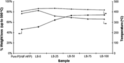
Atypical behaviors of BMIMTf ionic liquid present in ionic conductivity, SEM, and TG/DTG analyses of P(VdF-HFP)/LiTf-based solid polymer electrolyte system
-
- Journal:
- Journal of Materials Research / Volume 26 / Issue 23 / 14 December 2011
- Published online by Cambridge University Press:
- 08 November 2011, pp. 2945-2951
- Print publication:
- 14 December 2011
-
- Article
- Export citation

Bending manipulation and measurements of fracture strength of silicon and oxidized silicon nanowires by atomic force microscopy
-
- Journal:
- Journal of Materials Research / Volume 27 / Issue 3 / 14 February 2012
- Published online by Cambridge University Press:
- 08 November 2011, pp. 562-570
- Print publication:
- 14 February 2012
-
- Article
- Export citation

Improved structural and electrical properties of thin ZnO:Al films by dc filtered cathodic arc deposition
-
- Journal:
- Journal of Materials Research / Volume 27 / Issue 5 / 14 March 2012
- Published online by Cambridge University Press:
- 07 November 2011, pp. 857-862
- Print publication:
- 14 March 2012
-
- Article
- Export citation
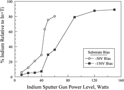
Structural and tribological characterization of Ti–In–N films deposited by magnetron sputter deposition
-
- Journal:
- Journal of Materials Research / Volume 27 / Issue 5 / 14 March 2012
- Published online by Cambridge University Press:
- 07 November 2011, pp. 850-856
- Print publication:
- 14 March 2012
-
- Article
- Export citation

Nanotribological and nanomechanical properties of plasma-polymerized polyterpenol thin films
-
- Journal:
- Journal of Materials Research / Volume 26 / Issue 23 / 14 December 2011
- Published online by Cambridge University Press:
- 04 November 2011, pp. 2952-2961
- Print publication:
- 14 December 2011
-
- Article
- Export citation

Conceptual progress for explaining and predicting semiconductor properties
-
- Journal:
- Journal of Materials Research / Volume 26 / Issue 22 / 28 November 2011
- Published online by Cambridge University Press:
- 04 November 2011, pp. 2815-2825
- Print publication:
- 28 November 2011
-
- Article
- Export citation

A brittleness transition in silicon due to scale
-
- Journal:
- Journal of Materials Research / Volume 27 / Issue 3 / 14 February 2012
- Published online by Cambridge University Press:
- 04 November 2011, pp. 552-561
- Print publication:
- 14 February 2012
-
- Article
- Export citation

Predation versus protection: Fish teeth and scales evaluated by nanoindentation
-
- Journal:
- Journal of Materials Research / Volume 27 / Issue 1 / 14 January 2012
- Published online by Cambridge University Press:
- 04 November 2011, pp. 100-112
- Print publication:
- 14 January 2012
-
- Article
- Export citation

Half-Heusler phases and nanocomposites as emerging high-ZT thermoelectric materials
-
- Journal:
- Journal of Materials Research / Volume 26 / Issue 22 / 28 November 2011
- Published online by Cambridge University Press:
- 04 November 2011, pp. 2795-2802
- Print publication:
- 28 November 2011
-
- Article
- Export citation
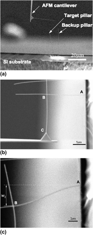
Size effects on deformation mechanism of nanopillars by FIB-CVD using double-cantilever testing
-
- Journal:
- Journal of Materials Research / Volume 27 / Issue 3 / 14 February 2012
- Published online by Cambridge University Press:
- 04 November 2011, pp. 521-527
- Print publication:
- 14 February 2012
-
- Article
- Export citation

On-chip tensile testing of nanoscale silicon free-standing beams
-
- Journal:
- Journal of Materials Research / Volume 27 / Issue 3 / 14 February 2012
- Published online by Cambridge University Press:
- 04 November 2011, pp. 571-579
- Print publication:
- 14 February 2012
-
- Article
- Export citation
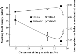
Influence of Co content on stacking fault energy in Ni–Co base disk superalloys
-
- Journal:
- Journal of Materials Research / Volume 26 / Issue 22 / 28 November 2011
- Published online by Cambridge University Press:
- 04 November 2011, pp. 2833-2837
- Print publication:
- 28 November 2011
-
- Article
- Export citation

Modeling of kinetic and static friction between an elastically bent nanowire and a flat surface
-
- Journal:
- Journal of Materials Research / Volume 27 / Issue 3 / 14 February 2012
- Published online by Cambridge University Press:
- 04 November 2011, pp. 580-585
- Print publication:
- 14 February 2012
-
- Article
- Export citation
Plasticity-induced oxidation reactivity on Ni(100) studied by scanning tunneling spectroscopy – CORRIGENDUM
-
- Journal:
- MRS Communications / Volume 2 / Issue 1 / March 2012
- Published online by Cambridge University Press:
- 04 November 2011, p. 29
- Print publication:
- March 2012
-
- Article
-
- You have access
- HTML
- Export citation
