Refine search
Actions for selected content:
106117 results in Materials Science
PDJ volume 29 issue 3 Cover and Front matter
-
- Journal:
- Powder Diffraction / Volume 29 / Issue 3 / September 2014
- Published online by Cambridge University Press:
- 30 September 2014, pp. f1-f6
-
- Article
-
- You have access
- Export citation
Powder Diffraction: Here for you now and in the future
-
- Journal:
- Powder Diffraction / Volume 29 / Issue 3 / September 2014
- Published online by Cambridge University Press:
- 30 September 2014, p. 219
-
- Article
-
- You have access
- HTML
- Export citation

Microcantilever bending experiments in NiAl – Evaluation, size effects, and crack tip plasticity
-
- Journal:
- Journal of Materials Research / Volume 29 / Issue 18 / 28 September 2014
- Published online by Cambridge University Press:
- 26 September 2014, pp. 2129-2140
- Print publication:
- 28 September 2014
-
- Article
- Export citation
-
For a better understanding of the local fracture behavior of semi-brittle materials, we carried out bending experiments on notched microcantilevers of varying sizes in the micrometer range using NiAl single crystals. Smaller and larger beams were milled with a focused ion beam in the so-called “soft” <110> and “hard” <100> orientation and were tested in situ in a scanning electron microscope and ex situ with a nanoindenter, respectively. The measurements were evaluated using both linear-elastic fracture mechanics and elastic–plastic fracture mechanics. The results show that (i) the fracture toughness is in the same range as the macroscopically determined one which is around 3.5 MPa $\sqrt {\rm{m}}$ for the soft orientation and around 8.5 MPa $\sqrt {\rm{m}}$ for the hard orientation, that (ii) there is a strong influence of the anisotropic behavior of NiAl on the fracture toughness values, and that (iii) the J-integral technique is the most accurate quantification method.


JMR volume 29 issue 18 Cover and Front matter
-
- Journal:
- Journal of Materials Research / Volume 29 / Issue 18 / 28 September 2014
- Published online by Cambridge University Press:
- 26 September 2014, pp. f1-f5
- Print publication:
- 28 September 2014
-
- Article
-
- You have access
- Export citation

Improvement of carbon nanocoil purity achieved by supplying catalyst molecules from the vapor phase in chemical vapor deposition
-
- Journal:
- Journal of Materials Research / Volume 29 / Issue 18 / 28 September 2014
- Published online by Cambridge University Press:
- 26 September 2014, pp. 2179-2187
- Print publication:
- 28 September 2014
-
- Article
- Export citation

Methanol desorption in poly(methyl methacrylate) with stress distributions
-
- Journal:
- Journal of Materials Research / Volume 29 / Issue 18 / 28 September 2014
- Published online by Cambridge University Press:
- 26 September 2014, pp. 2162-2169
- Print publication:
- 28 September 2014
-
- Article
- Export citation

Influence of heat treatment on the microstructure and corrosion behavior of Ni–Fe–Cr alloy 028
-
- Journal:
- Journal of Materials Research / Volume 29 / Issue 18 / 28 September 2014
- Published online by Cambridge University Press:
- 26 September 2014, pp. 2147-2155
- Print publication:
- 28 September 2014
-
- Article
- Export citation
JMR volume 29 issue 18 Cover and Back matter
-
- Journal:
- Journal of Materials Research / Volume 29 / Issue 18 / 28 September 2014
- Published online by Cambridge University Press:
- 26 September 2014, pp. b1-b5
- Print publication:
- 28 September 2014
-
- Article
-
- You have access
- Export citation

Microstructure and mechanical properties of electrodeposited Al1−x Mnx /Al1−y Mny nanostructured multilayers
-
- Journal:
- Journal of Materials Research / Volume 29 / Issue 18 / 28 September 2014
- Published online by Cambridge University Press:
- 26 September 2014, pp. 2229-2239
- Print publication:
- 28 September 2014
-
- Article
-
- You have access
- HTML
- Export citation

Highly uniform arrays of epitaxial Ge quantum dots with interdot spacing of 50 nm
-
- Journal:
- Journal of Materials Research / Volume 29 / Issue 18 / 28 September 2014
- Published online by Cambridge University Press:
- 26 September 2014, pp. 2240-2249
- Print publication:
- 28 September 2014
-
- Article
-
- You have access
- HTML
- Export citation

One-pot polyelectrolyte assisted hydrothermal synthesis of NiFe2O4-reduced graphene oxide nanocomposites with improved electrochemical and photocatalytic properties
-
- Journal:
- Journal of Materials Research / Volume 29 / Issue 18 / 28 September 2014
- Published online by Cambridge University Press:
- 26 September 2014, pp. 2211-2219
- Print publication:
- 28 September 2014
-
- Article
- Export citation
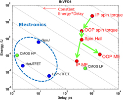
Benchmarking spintronic logic devices based on magnetoelectric oxides
-
- Journal:
- Journal of Materials Research / Volume 29 / Issue 18 / 28 September 2014
- Published online by Cambridge University Press:
- 26 September 2014, pp. 2109-2115
- Print publication:
- 28 September 2014
-
- Article
- Export citation
12 - Gate metals
- from Part III - Real MOS systems
-
- Book:
- The MOS System
- Published online:
- 05 October 2014
- Print publication:
- 25 September 2014, pp 297-307
-
- Chapter
- Export citation
Part II - Characterization techniques
-
- Book:
- The MOS System
- Published online:
- 05 October 2014
- Print publication:
- 25 September 2014, pp 129-130
-
- Chapter
- Export citation
14 - MOS systems on high-mobility channel materials
- from Part III - Real MOS systems
-
- Book:
- The MOS System
- Published online:
- 05 October 2014
- Print publication:
- 25 September 2014, pp 333-351
-
- Chapter
- Export citation
1 - Introduction
-
- Book:
- The MOS System
- Published online:
- 05 October 2014
- Print publication:
- 25 September 2014, pp 1-8
-
- Chapter
- Export citation
Index
-
- Book:
- The MOS System
- Published online:
- 05 October 2014
- Print publication:
- 25 September 2014, pp 352-355
-
- Chapter
- Export citation
5 - Carrier capture at bulk oxide traps
- from Part I - Basic properties
-
- Book:
- The MOS System
- Published online:
- 05 October 2014
- Print publication:
- 25 September 2014, pp 104-128
-
- Chapter
- Export citation
Preface
-
-
- Book:
- The MOS System
- Published online:
- 05 October 2014
- Print publication:
- 25 September 2014, pp xi-xii
-
- Chapter
- Export citation
13 - Transmission probabilities and current leakage in gate oxides
- from Part III - Real MOS systems
-
- Book:
- The MOS System
- Published online:
- 05 October 2014
- Print publication:
- 25 September 2014, pp 308-332
-
- Chapter
- Export citation
