Refine search
Actions for selected content:
106117 results in Materials Science
Nanoimprint lithographic surface patterning of sol–gel fabricated nickel ferrite (NiFe2O4) – ERRATUM
-
- Journal:
- MRS Communications / Volume 4 / Issue 4 / December 2014
- Published online by Cambridge University Press:
- 25 September 2014, p. 195
- Print publication:
- December 2014
-
- Article
-
- You have access
- HTML
- Export citation
11 - MOS systems with high-k dielectrics
- from Part III - Real MOS systems
-
- Book:
- The MOS System
- Published online:
- 05 October 2014
- Print publication:
- 25 September 2014, pp 261-296
-
- Chapter
- Export citation
Frontmatter
-
- Book:
- The MOS System
- Published online:
- 05 October 2014
- Print publication:
- 25 September 2014, pp i-iv
-
- Chapter
- Export citation
10 - MOS systems with silicon dioxide dielectrics
- from Part III - Real MOS systems
-
- Book:
- The MOS System
- Published online:
- 05 October 2014
- Print publication:
- 25 September 2014, pp 231-260
-
- Chapter
- Export citation
Contents
-
- Book:
- The MOS System
- Published online:
- 05 October 2014
- Print publication:
- 25 September 2014, pp v-x
-
- Chapter
- Export citation
Part I - Basic properties
-
- Book:
- The MOS System
- Published online:
- 05 October 2014
- Print publication:
- 25 September 2014, pp 9-10
-
- Chapter
- Export citation
3 - Basic properties of the gate stack
- from Part I - Basic properties
-
- Book:
- The MOS System
- Published online:
- 05 October 2014
- Print publication:
- 25 September 2014, pp 32-70
-
- Chapter
- Export citation
4 - Electron states at MOS interfaces
- from Part I - Basic properties
-
- Book:
- The MOS System
- Published online:
- 05 October 2014
- Print publication:
- 25 September 2014, pp 71-103
-
- Chapter
- Export citation
7 - Electrical characterization by thermal activation
- from Part II - Characterization techniques
-
- Book:
- The MOS System
- Published online:
- 05 October 2014
- Print publication:
- 25 September 2014, pp 168-195
-
- Chapter
- Export citation
8 - Characterization of oxide/silicon energy band alignment: internal photoemission and X-ray photoelectron spectroscopy
- from Part II - Characterization techniques
-
- Book:
- The MOS System
- Published online:
- 05 October 2014
- Print publication:
- 25 September 2014, pp 196-220
-
- Chapter
- Export citation
2 - Basic properties of the MOS system
- from Part I - Basic properties
-
- Book:
- The MOS System
- Published online:
- 05 October 2014
- Print publication:
- 25 September 2014, pp 11-31
-
- Chapter
- Export citation
9 - Electron spin-based methods
- from Part II - Characterization techniques
-
- Book:
- The MOS System
- Published online:
- 05 October 2014
- Print publication:
- 25 September 2014, pp 221-228
-
- Chapter
- Export citation
6 - Electrical characterization by Fermi-probe technique
- from Part II - Characterization techniques
-
- Book:
- The MOS System
- Published online:
- 05 October 2014
- Print publication:
- 25 September 2014, pp 131-167
-
- Chapter
- Export citation
Part III - Real MOS systems
-
- Book:
- The MOS System
- Published online:
- 05 October 2014
- Print publication:
- 25 September 2014, pp 229-230
-
- Chapter
- Export citation
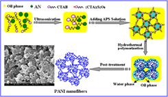
Interconnected polyaniline clusters constructed from nanowires: Confined polymerization and electrochemical properties
-
- Journal:
- Journal of Materials Research / Volume 29 / Issue 20 / 28 October 2014
- Published online by Cambridge University Press:
- 24 September 2014, pp. 2408-2415
- Print publication:
- 28 October 2014
-
- Article
- Export citation

Preparation of TiNi films by diffusion technology and the study of the formation sequence of the intermetallics in Ti–Ni systems
-
- Journal:
- Journal of Materials Research / Volume 29 / Issue 22 / 28 November 2014
- Published online by Cambridge University Press:
- 24 September 2014, pp. 2707-2716
- Print publication:
- 28 November 2014
-
- Article
- Export citation
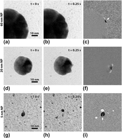
Physical response of gold nanoparticles to single self-ion bombardment
-
- Journal:
- Journal of Materials Research / Volume 29 / Issue 20 / 28 October 2014
- Published online by Cambridge University Press:
- 23 September 2014, pp. 2387-2397
- Print publication:
- 28 October 2014
-
- Article
- Export citation

Fluorescent π-conjugated polymer nanoparticles: A new synthetic approach based on nanoagglomeration via polyion association
-
- Journal:
- Journal of Materials Research / Volume 30 / Issue 1 / 14 January 2015
- Published online by Cambridge University Press:
- 23 September 2014, pp. 10-18
- Print publication:
- 14 January 2015
-
- Article
- Export citation
Improvements in microstructure and mechanical properties of Al–Si–Cu alloy–Al2O3 nanocomposite modified by ZrO2
-
- Journal:
- Journal of Materials Research / Volume 29 / Issue 21 / 14 November 2014
- Published online by Cambridge University Press:
- 23 September 2014, pp. 2505-2513
- Print publication:
- 14 November 2014
-
- Article
- Export citation
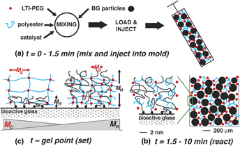
Investigating the effects of surface-initiated polymerization of ε-caprolactone to bioactive glass particles on the mechanical properties of settable polymer/ceramic composites
-
- Journal:
- Journal of Materials Research / Volume 29 / Issue 20 / 28 October 2014
- Published online by Cambridge University Press:
- 18 September 2014, pp. 2398-2407
- Print publication:
- 28 October 2014
-
- Article
- Export citation
