To save content items to your account,
please confirm that you agree to abide by our usage policies.
If this is the first time you use this feature, you will be asked to authorise Cambridge Core to connect with your account.
Find out more about saving content to .
To save content items to your Kindle, first ensure no-reply@cambridge.org
is added to your Approved Personal Document E-mail List under your Personal Document Settings
on the Manage Your Content and Devices page of your Amazon account. Then enter the ‘name’ part
of your Kindle email address below.
Find out more about saving to your Kindle.
Note you can select to save to either the @free.kindle.com or @kindle.com variations.
‘@free.kindle.com’ emails are free but can only be saved to your device when it is connected to wi-fi.
‘@kindle.com’ emails can be delivered even when you are not connected to wi-fi, but note that service fees apply.
Optical neural interfaces offer several advantages over electrophysiological methods in both clinical and experimental applications. Optical stimulation techniques exhibit high spatial selectivity, do not create electrical artifacts, and allow for stimulation of specific neuronal populations. Calcium- and voltage-sensitive dyes can probe neuronal and astrocytic signaling at both single cell and network scales, and miniature optical sensors can measure a variety of physiological signals in situ. However, optical neural interfaces must be robust, safe, and effective over long periods of time in order to be acceptable for use in human patients. In this article, we draw the attention of the materials science community to the need for a new generation of materials that have the necessary optical performance and, at the same time, conform to the constraints placed on implanted devices in terms of size, relevant mechanical properties, and biocompatibility, providing some examples of recent advancements in the field.
Multi-fingered prosthetic limbs are now capable of performing complex movements, closely simulating those of the lost human arm/hand in amputees. Conveying natural control and perception of such sophisticated robotic limbs requires direct interfacing with the nervous system of the users. Both the brain and transected peripheral nerves have been proposed as appropriate locations for such neural interfaces. In the peripheral nerves, several electrode designs have been used successfully to record motor signals, and through stimulation, used to convey sensation in long-term amputee human volunteers. Here we review the advantages and limitations of peripheral nerve interfaces (PNIs) in relation to the desired characteristics for safety and performance. We compare current PNI electrodes and materials designed to increase recording sensitivity and to achieve selective stimulation of different nerves such as those carrying mechanical sensation and limb position information. Emphasis is placed on novel electrode materials, including biological coatings, conductive polymers, and nanostructured modifications. Successful development of reliable PNIs will not only enable natural control and feel of future robotic prosthetics, but will likely be a centerpiece technology in the development of multiple bionic organs.
The treatment of disorders of the nervous system poses a major clinical challenge. Development of neuromodulation (i.e., interfacing electronics to nervous tissue to modulate its function) has provided patients with neuronal-related deficits a new tool to regain lost function. Even though, in principle, electrical stimulation and recording by interfacing technology is simple and straightforward, each presents different challenges. In stimulation, the challenge lies in targeting the effects of stimulation on precise brain regions, as each region specializes for particular functions on a millimeter scale. In practice, our experience with deep brain stimulation for treating Parkinson’s disease reveals that stimulation of larger regions of the brain can be relatively well tolerated. However, the task of fabricating an ideal electrode that performs reliably for long periods of time has been daunting. The primary obstacle in successful interfacing comes from integration of electrodes (“foreign” material) into the nervous system (biological material). The second tier of complexity is added by the need for the electrodes to “sense” signals emanating from individual neurons, an estimated microenvironment of 10 to 20 microns in diameter. Materials design and technology impact electrode design—with their size, shape, mechanical properties, and composition all being actively optimized to enable chronic, stable recordings of neural activity. The articles in this issue discuss designing interfacing technology to “listen to the nervous system” from a materials perspective. These include identification of materials with a potential for in vivo development, electrodes with various material types, including natural nanocomposites, and optical neural interfacing.
LiMn2O4 nanowires have been synthesized by a two-step approach. γ-MnOOH nanowires are firstly synthesized by hydrothermal method and after further sintering with LiOH at 750 °C for about 3 h, the wire-like LiMn2O4 can be obtained. The structure of the final product is characterized by x-ray diffraction using Rietveld refinement. Its electrochemical performance is investigated by galvanostatic tests. The as-prepared LiMn2O4 nanowires display excellent cyclability. The LiMn2O4 nanowires with good cycle stability may be beneficial from the structural stability of LiMn2O4 crystal cell and one-dimensional nanostructure.
Oxidation kinetics of copper nanowires (CuNWs) with diameter 25 ± 4 nm were studied. The dry powder of CuNWs before oxidation comprises 73.2 wt% Cu and 26.8 wt% Cu2O. The oxidation reaction can be divided into two stages at weight of 111.2%. Oxidized CuNWs after Stage 1 consist of Cu2O and CuO. Oxidized CuNWs after Stage 2 comprise CuO only. The activation energies for both stages are determined by Kissinger method and other five isoconversional methods: Flynn–Wall–Osawa, Starink, Kissinger–Akahira–Sunose, Boswell and Friedman differential methods. The isoconversional activation energies determined by Starink method are used to fit different master plots. The Johnson–Mehl–Avrami equation gives the best fit. Surface atoms are the sites for the random nucleation, and the crystallite strain in CuNWs is the driving force for the growth of nuclei during the oxidation process.
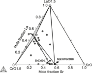
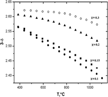
The thermodynamic La–Sr–Mn–Cr–O oxide database is obtained as an extension of thermodynamic descriptions of oxide subsystems using the calculation of phase diagrams approach. Concepts of the thermodynamic modeling of solid oxide phases are discussed. Gibbs energy functions of SrCrO4, Sr2.67Cr2O8, Sr2CrO4, and SrCr2O4 are presented, and thermodynamic model parameters of La–Sr–Mn–Chromite perovskite are given. Experimental solid solubilities and nonstoichiometries in La1−xSrxCrO3−δ and LaMn1−xCrxO3−δ are reproduced by the model. The presented oxide database can be used for applied computational thermodynamics of traditional lanthanum manganite cathode with Cr-impurities. It represents the fundament for extensions to higher orders, aiming on thermodynamic calculations in noble symmetric solid oxide fuel cells.
Samples with overall composition HoxSr1−xCoO3−δ within the range 0.05 ≤ x ≤ 0.9 were prepared by a solid-state technique at 1100 °C in air. Single-phase HoxSr1−xCoO3−δ oxides were obtained within the range 0.05 ≤ x ≤ 0.30. Solid solutions of Ho0.05Sr0.95CoO3−δ and Ho0.1Sr0.9CoO3−δ were indexed in the cubic structure (Pm3m sp. gr.) with the unit cell parameters a = 3.846 Å and a = 3.842 Å, respectively. Further introduction of holmium leads to a change of crystal structure from cubic to a tetragonal 2ap × 2ap × 4ap superstructure. All samples with x > 0.3 were multiphase, containing a saturated solid solution with approximate composition Ho0.3Sr0.7CoO3−δ with Ho2O3 and CoO. The change of oxygen nonstoichiometry was measured by thermogravimetric analysis within the temperature range 25 ≤ T (°C) ≤ 1100. The absolute value of oxygen nonstoichiometry was calculated from the results of chromatometric titration. Thermal expansion coefficients of Ho1−xSrxCoO3−δ were measured by dilatometry within the temperature range 25 ≤ T (°C) ≤ 1100 in air.
The structural, mechanical, and electronic properties of rhenium, osmium, and tungsten tetranitrides, XN4 (X = Re, Os, W) with the orthorhombic ReP4-type structure have been investigated by first-principles calculations using density functional plane-wave pseudopotential method. The calculated formation enthalpies and elastic constants show that these tetranitrides are energetically and mechanically stable. It is appeared from the calculated band structures and density of states that ReN4 and new proposed WN4 are metallic, while OsN4 is semiconductor with a band gap of 0.64 eV. The hardness values of all compounds obtained from different hardness methods indicate that these tetranitrides are superhard materials.
Nanocomposite Zr0.52Al0.48N1.11 thin films consisting of crystalline grains surrounded by an amorphous matrix were deposited using cathodic arc evaporation. The structure evolution after annealing of the films was studied using high-energy x-ray scattering and transmission electron microscopy. The mechanical properties were characterized by nanoindentation on as-deposited and annealed films. After annealing in temperatures of 1050–1400 °C, nucleation and grain growth of cubic ZrN takes place in the film. This increases the hardness, which reaches a maximum, while parts of the film remain amorphous. Grain growth of the hexagonal AlN phase occurs above 1300 °C.
Plasticity initiation behavior that appears as a pop-in phenomenon on a loading process during indentation-induced deformation was investigated to reveal the effects of lattice defects such as grain boundary and solute element for various metallic materials including Fe alloys through instrumented nanoindentation techniques. The critical load Pc of pop-in on a loading process is lower in the vicinity of the grain boundary than in the grain interior, but the relative hardness of the boundary is equal to or greater than that in grain interior. In-solution Si produces a larger increase in the Pc for both the grain boundary and the grain interior in the Fe–Si alloy than in the interstitial-free steel. The maximum shear stress corresponding to the Pc underneath the indenter is directly proportional to the shear modulus in single crystals with various crystallographic structures. Microstructural effects on the Pc are considered based on some dislocation models.
Mesoporous titanium dioxide (TiO2) and lithium (Li)-doped TiO2 nanobelts were synthesized via a facile solvothermal process. The crystalline structure and morphology of the nanobelts were characterized in detail. The x-ray diffraction patterns, transmission electron microscopy (TEM) and high-resolution TEM (HRTEM) images indicate that the nanobelts have uniform monoclinic geometry with a length of 3–4 μm and a width of 40–200 nm, the pores are also uniform with 5–7 nm in diameter. scanning electron microscopy and TEM studies demonstrate the as-prepared TiO2 nanobelts have varied morphologies that strongly depend on the volume ratio of the reaction medium and the pressure. Ultraviolet-visible diffuse reflectance spectroscopy was used to study the photocatalytic degradation of Malachite green over the lithium nanoparticle-loaded mesoporous TiO2 nanobelts. The doping of lithium does not change the crystalline phase but the results form infrared spectrums confirm that the Li+ ion incorporates into the lattice of TiO2 nanobelts, decomposes it by replacing Ti4+ and thus reduces the photocatalytic activity.
Many-body perturbation theory is applied to compute the quasiparticle electronic structures and the optical absorption spectra (including excitonic effects) for several transparent conducting oxides (TCOs). We discuss HSE+G0W0 results (based on the hybrid exchange-correlation functional by Heyd, Scuseria, and Ernzerhof, and quasiparticle corrections from approximating the electronic self energy as the product of the Green’s function and the screened Coulomb interaction) for band structures, fundamental band gaps, and effective electron masses of magnesium oxide, zinc oxide, cadmium oxide, tin dioxide, tin oxide, indium (III) oxide and silicon dioxide. The Bethe–Salpeter equation (BSE) is solved to account for excitonic effects in the calculation of the frequency-dependent absorption coefficients. We show that the HSE+G0W0 approach and the solution of the BSE are very well suited to describe the electronic structure and the optical properties of various TCOs in good agreement with experiment.
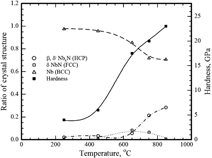
NbN thin films grown on Nb using pulsed laser deposition (PLD) were investigated for film crystal structures. The nanomechanical properties of NbN on Nb were examined as a function of the film/substrate crystal structure. X-ray diffraction (XRD) reveals peaks that correspond to δ-NbN cubic and β-Nb2N hexagonal phases in addition to δ′-NbN phase. Samples of various crystal structures were tested for phase characterization, microstructure, and surface morphology using XRD analysis, scanning electron microscopy, and atomic force microscopy. The nanomechanical properties were investigated using nanoindentation. The results indicate that there are clear effects of the crystal structure on the hardness of the PLD-grown NbNx films.
The present study aims to determine the optimum radio frequency (RF) sputtering power to obtain the desired W–TiO2 nanotubes for the best photoelectrochemical (PEC) performance. Tungsten (W) was deposited on titania (TiO2) nanotube arrays via RF sputtering technique under different sputtering powers from 50 to 250 W. The optimum content of W on TiO2 nanotube arrays play a significant role in maximizing the photocurrent generation efficiency to promote charge separation by accumulation of photogenerated electrons. The sputtering power below 180 W exhibited high-ordered and unbroken TiO2 nanotube arrays. However, the sputtering power over 180 W exhibited broken nanotube arrays and an oxide layer was formed due to the impact of high energy ions accelerated by a high sputtering power. The TiO2 nanotube arrays sputtered with tungsten at 50 W showed a better photocurrent density (1.55 mA/cm2), with a photoconversion efficiency of 2.2% in the PEC performance among the samples due to the effective charge separation and reduced recombination center in the resultant W–TiO2 nanotubes.
The migration mechanism and the minimum energy path of vacancies, interstitials, and an interstitial–vacancy pair in zinc oxide have been studied by the dimer method. The in-plane and out-of-plane migrations of zinc and oxygen vacancies are anisotropic. The kick-out mechanism is energetically preferred to zinc and oxygen interstitials that can easily migrate through the ZnO crystal lattice. In addition, the migration process of an interstitial–vacancy pair as a complex of an octahedral oxygen interstitial and a zinc vacancy is dominated by an oxygen interstitial/zinc vacancy successive migration. The energy barriers indicate that the existence of oxygen interstitial in the defect pair can promote the mobility of zinc vacancy, whereas the migration of oxygen interstitial is slowed down due to the presence of zinc vacancy. In the end, we show a possible migration path of the interstitial–vacancy pair that can be dissociated through a set of displacement movements.