Refine search
Actions for selected content:
212971 results in Engineering
Index
-
- Book:
- Introduction to Intelligent Systems, Control, and Machine Learning using MATLAB
- Published online:
- 27 November 2023
- Print publication:
- 16 November 2023, pp 470-472
-
- Chapter
- Export citation
Appendix G - Project Descriptions and Parts List
-
- Book:
- Introduction to Intelligent Systems, Control, and Machine Learning using MATLAB
- Published online:
- 27 November 2023
- Print publication:
- 16 November 2023, pp 467-469
-
- Chapter
- Export citation
5 - Incentivized Consensus Mechanism
- from Part II - Consensus Protocol Design in Blockchain Networks
-
- Book:
- Cryptoeconomics
- Published online:
- 06 January 2024
- Print publication:
- 16 November 2023, pp 67-94
-
- Chapter
- Export citation

Dual scaling and the n-thirds law in grid turbulence
-
- Journal:
- Journal of Fluid Mechanics / Volume 975 / 25 November 2023
- Published online by Cambridge University Press:
- 16 November 2023, A32
-
- Article
- Export citation
-
A dual scaling of the turbulent longitudinal velocity structure function
 $\overline {{(\delta u)}^n}$, i.e. a scaling based on the Kolmogorov scales (
 $u_K$,
  $\eta$) and another based on (
 $u'$,
$u'$,  $L$) representative of the large scale motion, is examined in the context of both the Kármán–Howarth equation and experimental grid turbulence data over a significant range of the Taylor microscale Reynolds number
  $Re_\lambda$. As
  $Re_\lambda$ increases, the scaling based on (
 $u'$,
$u'$,  $L$) extends to increasingly smaller values of
  $r/L$ while the scaling based on (
 $u_K$,
  $\eta$) extends to increasingly larger values of
  $r/\eta$. The implication is that both scalings should eventually overlap in the so-called inertial range as
  $Re_\lambda$ continues to increase, thus leading to a power-law relation
  $\overline {{(\delta u)}^n} \sim r^{n/3}$ when the inertial range is rigorously established. The latter is likely to occur only when
  $Re_\lambda \to \infty$. The use of an empirical model for
  $\overline {{(\delta u)}^n}$, which complies with
  $\overline {{(\delta u)}^n} \sim r^{n/3}$ as
  $Re_\lambda \to \infty$, shows that the finite Reynolds number effect may differ between even- and odd-orders of
  $\overline {{(\delta u)}^n}$. This suggests that different values of
  $Re_\lambda$ may be required between even and odd values of
  $n$ for compliance with
  $\overline {{(\delta u)}^n} \sim r^{n/3}$. The model describes adequately the dependence on
  $Re_\lambda$ of the available experimental data for
  $\overline {{(\delta u)}^n}$ and supports indirectly the extrapolation of these data to infinitely large
  $Re_\lambda$.


Contents
-
- Book:
- Introduction to Intelligent Systems, Control, and Machine Learning using MATLAB
- Published online:
- 27 November 2023
- Print publication:
- 16 November 2023, pp vii-xii
-
- Chapter
- Export citation
Preface
-
- Book:
- Integrated Circuit Fabrication
- Published online:
- 01 December 2023
- Print publication:
- 16 November 2023, pp xiii-xvi
-
- Chapter
- Export citation
A.6 - Properties of Insulators Used in Semiconductor Technology
- from Appendices
-
- Book:
- Integrated Circuit Fabrication
- Published online:
- 01 December 2023
- Print publication:
- 16 November 2023, pp 645-645
-
- Chapter
- Export citation
A.5 - Physical Properties of Silicon
- from Appendices
-
- Book:
- Integrated Circuit Fabrication
- Published online:
- 01 December 2023
- Print publication:
- 16 November 2023, pp 644-644
-
- Chapter
- Export citation
11 - Back-End (Interconnect) Processing Technologies
-
- Book:
- Integrated Circuit Fabrication
- Published online:
- 01 December 2023
- Print publication:
- 16 November 2023, pp 551-618
-
- Chapter
- Export citation

Wave statistics and energy dissipation of shallow-water breaking waves in a tank with a level bottom
-
- Journal:
- Journal of Fluid Mechanics / Volume 975 / 25 November 2023
- Published online by Cambridge University Press:
- 16 November 2023, A25
-
- Article
-
- You have access
- Open access
- HTML
- Export citation
-
The present study focuses on two-dimensional direct numerical simulations of shallow-water breaking waves, specifically those generated by a wave plate at constant water depths. The primary objective is to quantitatively analyse the dynamics, kinematics and energy dissipation associated with wave breaking. The numerical results exhibit good agreement with experimental data in terms of free-surface profiles during wave breaking. A parametric study was conducted to examine the influence of various wave properties and initial conditions on breaking characteristics. According to research on the Bond number (
 $Bo$, the ratio of gravitational to surface tension forces), an increased surface tension leads to the formation of more prominent parasitic capillaries at the forwards face of the wave profile and a thicker plunging jet, which causes a delayed breaking time and is tightly correlated with the main cavity size. A close relationship between wave statistics and the initial conditions of the wave plate is discovered, allowing for the classification of breaker types based on the ratio of wave height to water depth,
  $H/d$. Moreover, an analysis based on inertial scaling arguments reveals that the energy dissipation rate due to breaking can be linked to the local geometry of the breaking crest
  $H_b/d$, and exhibits a threshold behaviour, where the energy dissipation approaches zero at a critical value of
  $H_b/d$. An empirical scaling of the breaking parameter is proposed as
 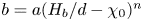 $b = a(H_b/d - \chi _0)^n$, where
  $\chi _0 = 0.65$ represents the breaking threshold and
  $n = 1.5$ is a power law determined through the best fit to the numerical results.


Appendix E - Introduction to Arduino Microcontrollers
-
- Book:
- Introduction to Intelligent Systems, Control, and Machine Learning using MATLAB
- Published online:
- 27 November 2023
- Print publication:
- 16 November 2023, pp 459-462
-
- Chapter
- Export citation
6 - Mechanism Design Basics
- from Part III - Mechanism Design in Blockchain Networks and Beyond
-
- Book:
- Cryptoeconomics
- Published online:
- 06 January 2024
- Print publication:
- 16 November 2023, pp 97-133
-
- Chapter
- Export citation
Appendices
-
- Book:
- Integrated Circuit Fabrication
- Published online:
- 01 December 2023
- Print publication:
- 16 November 2023, pp 619-656
-
- Chapter
- Export citation
Design and analysis of an energy selective rasorber – CORRIGENDUM
-
- Journal:
- International Journal of Microwave and Wireless Technologies / Volume 16 / Issue 2 / March 2024
- Published online by Cambridge University Press:
- 16 November 2023, p. 357
-
- Article
-
- You have access
- HTML
- Export citation
10 - Open Questions about Mechanism Design in Cryptoeconomics
- from Part IV - Open Questions of Cryptoeconomics
-
- Book:
- Cryptoeconomics
- Published online:
- 06 January 2024
- Print publication:
- 16 November 2023, pp 245-254
-
- Chapter
- Export citation
FLM volume 974 Cover and Front matter
-
- Journal:
- Journal of Fluid Mechanics / Volume 974 / 10 November 2023
- Published online by Cambridge University Press:
- 16 November 2023, p. f1
-
- Article
-
- You have access
- Export citation
Appendices
-
- Book:
- Introduction to Intelligent Systems, Control, and Machine Learning using MATLAB
- Published online:
- 27 November 2023
- Print publication:
- 16 November 2023, pp 375-469
-
- Chapter
- Export citation
6 - Semiconductor/Insulator Interfaces
-
- Book:
- Integrated Circuit Fabrication
- Published online:
- 01 December 2023
- Print publication:
- 16 November 2023, pp 255-309
-
- Chapter
- Export citation
A.2 - Standard Prefixes
- from Appendices
-
- Book:
- Integrated Circuit Fabrication
- Published online:
- 01 December 2023
- Print publication:
- 16 November 2023, pp 641-641
-
- Chapter
- Export citation
5 - Lithography
-
- Book:
- Integrated Circuit Fabrication
- Published online:
- 01 December 2023
- Print publication:
- 16 November 2023, pp 159-254
-
- Chapter
- Export citation
