Refine search
Actions for selected content:
106129 results in Materials Science
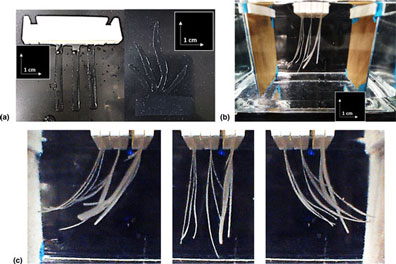
Cellulose-based electroactive hydrogels for seaweed mimicking toward hybrid artificial habitats creation
-
- Journal:
- MRS Communications / Volume 8 / Issue 3 / September 2018
- Published online by Cambridge University Press:
- 15 August 2018, pp. 1129-1134
- Print publication:
- September 2018
-
- Article
- Export citation
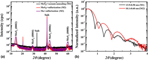
Atomic-level insights through spectroscopic and transport measurements into the large-area synthesis of MoS2 thin films
-
- Journal:
- MRS Communications / Volume 8 / Issue 3 / September 2018
- Published online by Cambridge University Press:
- 15 August 2018, pp. 1328-1334
- Print publication:
- September 2018
-
- Article
- Export citation
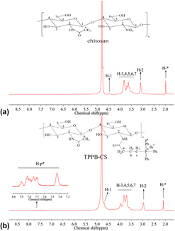
Antitumor activity and antitumor mechanism of triphenylphosphonium chitosan against liver carcinoma
-
- Journal:
- Journal of Materials Research / Volume 33 / Issue 17 / 14 September 2018
- Published online by Cambridge University Press:
- 14 August 2018, pp. 2586-2597
- Print publication:
- 14 September 2018
-
- Article
- Export citation
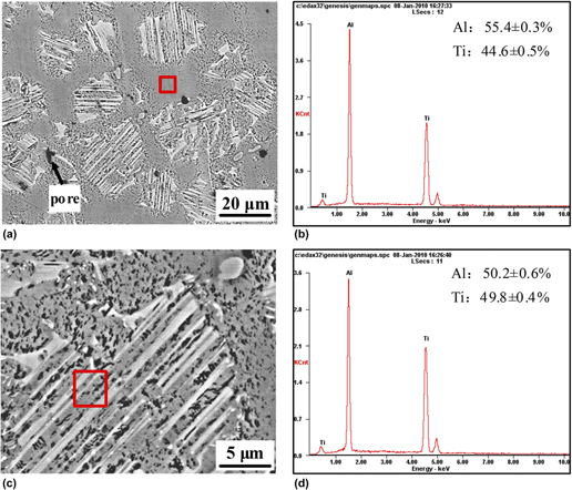
Microstructure evolution and hot deformation behavior of spray-deposited TiAl alloys
-
- Journal:
- Journal of Materials Research / Volume 33 / Issue 18 / 28 September 2018
- Published online by Cambridge University Press:
- 14 August 2018, pp. 2844-2852
- Print publication:
- 28 September 2018
-
- Article
- Export citation
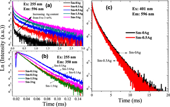
A significant enhancement emission of Sm3+–Ag+ codoped silicate glasses under UV excitation
-
- Journal:
- Journal of Materials Research / Volume 33 / Issue 16 / 28 August 2018
- Published online by Cambridge University Press:
- 14 August 2018, pp. 2434-2439
- Print publication:
- 28 August 2018
-
- Article
- Export citation
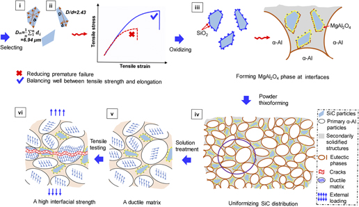
Toughening mechanisms of solution-treated SiCp/6061 aluminum matrix composites fabricated via powder thixoforming
-
- Journal:
- Journal of Materials Research / Volume 33 / Issue 18 / 28 September 2018
- Published online by Cambridge University Press:
- 14 August 2018, pp. 2728-2740
- Print publication:
- 28 September 2018
-
- Article
- Export citation
Compositional gradient films constructed by sputtering in a multicomponent Ti–Al–(Cr, Fe, Ni) system
-
- Journal:
- Journal of Materials Research / Volume 33 / Issue 19 / 14 October 2018
- Published online by Cambridge University Press:
- 14 August 2018, pp. 3330-3338
- Print publication:
- 14 October 2018
-
- Article
- Export citation
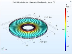
Finite element modeling of nanoscale-enabled microinductors for power electronics
-
- Journal:
- Journal of Materials Research / Volume 33 / Issue 15 / 13 August 2018
- Published online by Cambridge University Press:
- 13 August 2018, pp. 2223-2233
- Print publication:
- 13 August 2018
-
- Article
- Export citation
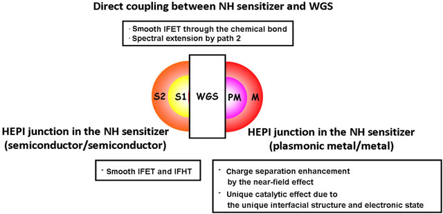
Nanohybrid-sensitized photoelectrochemical cells for solar-to-hydrogen conversion
-
- Journal:
- MRS Communications / Volume 8 / Issue 3 / September 2018
- Published online by Cambridge University Press:
- 13 August 2018, pp. 754-764
- Print publication:
- September 2018
-
- Article
- Export citation
JMR volume 33 issue 15 Cover and Back matter
-
- Journal:
- Journal of Materials Research / Volume 33 / Issue 15 / 13 August 2018
- Published online by Cambridge University Press:
- 13 August 2018, pp. b1-b5
- Print publication:
- 13 August 2018
-
- Article
-
- You have access
- Export citation
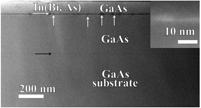
Microstructure of QD-like clusters in GaAs/In(As,Bi) heterosystems
-
- Journal:
- Journal of Materials Research / Volume 33 / Issue 16 / 28 August 2018
- Published online by Cambridge University Press:
- 13 August 2018, pp. 2342-2349
- Print publication:
- 28 August 2018
-
- Article
- Export citation
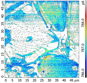
A novel approach to study the conductivity behavior of CaCu3Ti4O12 using scanning probe microscopy technique
-
- Journal:
- MRS Communications / Volume 8 / Issue 3 / September 2018
- Published online by Cambridge University Press:
- 13 August 2018, pp. 932-937
- Print publication:
- September 2018
-
- Article
- Export citation
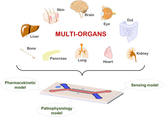
Multi-organ on a chip for personalized precision medicine
-
- Journal:
- MRS Communications / Volume 8 / Issue 3 / September 2018
- Published online by Cambridge University Press:
- 13 August 2018, pp. 652-667
- Print publication:
- September 2018
-
- Article
- Export citation
Stability of organic solar cells with PCDTBT donor polymer: An interlaboratory study – ERRATUM
-
- Journal:
- Journal of Materials Research / Volume 33 / Issue 16 / 28 August 2018
- Published online by Cambridge University Press:
- 13 August 2018, p. 2441
- Print publication:
- 28 August 2018
-
- Article
-
- You have access
- HTML
- Export citation

Direct visualization of nano and microscale polymer morphologies in as-prepared and dialyzed polyampholyte hydrogels by electron microscopy techniques
-
- Journal:
- MRS Communications / Volume 8 / Issue 3 / September 2018
- Published online by Cambridge University Press:
- 13 August 2018, pp. 1079-1084
- Print publication:
- September 2018
-
- Article
- Export citation

Observation and characterization of memristive silver filaments in amorphous zinc-tin-oxide
-
- Journal:
- MRS Communications / Volume 8 / Issue 3 / September 2018
- Published online by Cambridge University Press:
- 13 August 2018, pp. 1104-1110
- Print publication:
- September 2018
-
- Article
- Export citation
Introduction
-
- Journal:
- Journal of Materials Research / Volume 33 / Issue 15 / 13 August 2018
- Published online by Cambridge University Press:
- 13 August 2018, p. 2119
- Print publication:
- 13 August 2018
-
- Article
- Export citation
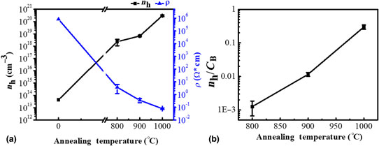
Boron doping of ultrananocrystalline diamond films by thermal diffusion process
-
- Journal:
- MRS Communications / Volume 8 / Issue 3 / September 2018
- Published online by Cambridge University Press:
- 13 August 2018, pp. 1111-1118
- Print publication:
- September 2018
-
- Article
- Export citation
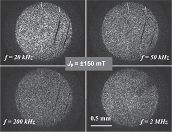
Characterization and assessment of the wideband magnetic properties of nanocrystalline alloys and soft ferrites
-
- Journal:
- Journal of Materials Research / Volume 33 / Issue 15 / 13 August 2018
- Published online by Cambridge University Press:
- 13 August 2018, pp. 2120-2137
- Print publication:
- 13 August 2018
-
- Article
- Export citation
JMR volume 33 issue 15 Cover and Front matter
-
- Journal:
- Journal of Materials Research / Volume 33 / Issue 15 / 13 August 2018
- Published online by Cambridge University Press:
- 13 August 2018, pp. f1-f4
- Print publication:
- 13 August 2018
-
- Article
-
- You have access
- Export citation
