Refine search
Actions for selected content:
106107 results in Materials Science
Materials for spin-transfer-torque magnetoresistive random-access memory
-
- Journal:
- MRS Bulletin / Volume 43 / Issue 5 / May 2018
- Published online by Cambridge University Press:
- 10 May 2018, pp. 352-357
- Print publication:
- May 2018
-
- Article
- Export citation
E-skin sensor self-heals and can be recycled
-
- Journal:
- MRS Bulletin / Volume 43 / Issue 5 / May 2018
- Published online by Cambridge University Press:
- 10 May 2018, p. 319
- Print publication:
- May 2018
-
- Article
-
- You have access
- HTML
- Export citation
2D Nanoelectronics: Physics and Devices of Atomically Thin Materials Mircea Dragoman and Daniela Dragoman
-
- Journal:
- MRS Bulletin / Volume 43 / Issue 5 / May 2018
- Published online by Cambridge University Press:
- 10 May 2018, p. 390
- Print publication:
- May 2018
-
- Article
-
- You have access
- HTML
- Export citation
MRS volume 43 issue 5 Cover and Front matter
-
- Journal:
- MRS Bulletin / Volume 43 / Issue 5 / May 2018
- Published online by Cambridge University Press:
- 10 May 2018, pp. f1-f7
- Print publication:
- May 2018
-
- Article
-
- You have access
- Export citation
European Commission to set up ethics committee on artificial intelligence
-
- Journal:
- MRS Bulletin / Volume 43 / Issue 5 / May 2018
- Published online by Cambridge University Press:
- 10 May 2018, pp. 326-327
- Print publication:
- May 2018
-
- Article
-
- You have access
- HTML
- Export citation
Hydrophobic and hydrophilic surfaces hold tight through chemical silane bonds
-
- Journal:
- MRS Bulletin / Volume 43 / Issue 5 / May 2018
- Published online by Cambridge University Press:
- 10 May 2018, p. 318
- Print publication:
- May 2018
-
- Article
-
- You have access
- HTML
- Export citation
US Academies examine open science and reproducibility
-
- Journal:
- MRS Bulletin / Volume 43 / Issue 5 / May 2018
- Published online by Cambridge University Press:
- 10 May 2018, pp. 325-326
- Print publication:
- May 2018
-
- Article
-
- You have access
- HTML
- Export citation
Electron Nano-Imaging: Basics of Imaging and Diffraction for TEM and STEM Nobuo Tanaka
-
- Journal:
- MRS Bulletin / Volume 43 / Issue 5 / May 2018
- Published online by Cambridge University Press:
- 10 May 2018, pp. 389-390
- Print publication:
- May 2018
-
- Article
-
- You have access
- HTML
- Export citation
Purely electronic nanometallic resistance switching random-access memory
-
- Journal:
- MRS Bulletin / Volume 43 / Issue 5 / May 2018
- Published online by Cambridge University Press:
- 10 May 2018, pp. 358-364
- Print publication:
- May 2018
-
- Article
-
- You have access
- HTML
- Export citation

Future of dynamic random-access memory as main memory
-
- Journal:
- MRS Bulletin / Volume 43 / Issue 5 / May 2018
- Published online by Cambridge University Press:
- 10 May 2018, pp. 334-339
- Print publication:
- May 2018
-
- Article
- Export citation
Atomic thin layers of Sn exhibit superconductivity
-
- Journal:
- MRS Bulletin / Volume 43 / Issue 5 / May 2018
- Published online by Cambridge University Press:
- 10 May 2018, p. 320
- Print publication:
- May 2018
-
- Article
-
- You have access
- HTML
- Export citation
Taking IMOS on the road—to Greece
-
- Journal:
- MRS Bulletin / Volume 43 / Issue 5 / May 2018
- Published online by Cambridge University Press:
- 10 May 2018, pp. 384-386
- Print publication:
- May 2018
-
- Article
-
- You have access
- HTML
- Export citation
In memoriam: Walter Lyons Brown
-
- Journal:
- MRS Bulletin / Volume 43 / Issue 5 / May 2018
- Published online by Cambridge University Press:
- 10 May 2018, p. 387
- Print publication:
- May 2018
-
- Article
-
- You have access
- HTML
- Export citation
Field-theoretic simulations: An emerging tool for probing soft material assembly
-
- Journal:
- MRS Bulletin / Volume 43 / Issue 5 / May 2018
- Published online by Cambridge University Press:
- 10 May 2018, pp. 371-378
- Print publication:
- May 2018
-
- Article
- Export citation
Bio Focus: Stretchable organic electronics on skin monitors health
-
- Journal:
- MRS Bulletin / Volume 43 / Issue 5 / May 2018
- Published online by Cambridge University Press:
- 10 May 2018, p. 321
- Print publication:
- May 2018
-
- Article
-
- You have access
- HTML
- Export citation
Spatially resolved texture and microstructure evolution of additively manufactured and gas gun deformed 304L stainless steel investigated by neutron diffraction and electron backscatter diffraction
-
- Journal:
- Powder Diffraction / Volume 33 / Issue 2 / June 2018
- Published online by Cambridge University Press:
- 30 April 2018, pp. 141-146
-
- Article
- Export citation
Geometry and algorithms to expand 2θ coverage of a 2D detector
-
- Journal:
- Powder Diffraction / Volume 33 / Issue 2 / June 2018
- Published online by Cambridge University Press:
- 30 April 2018, pp. 147-155
-
- Article
- Export citation
Improving ambient stability of BiI3-based perovskites using different phosphoniums as the organic cation
-
- Journal:
- MRS Communications / Volume 8 / Issue 3 / September 2018
- Published online by Cambridge University Press:
- 30 April 2018, pp. 878-884
- Print publication:
- September 2018
-
- Article
- Export citation
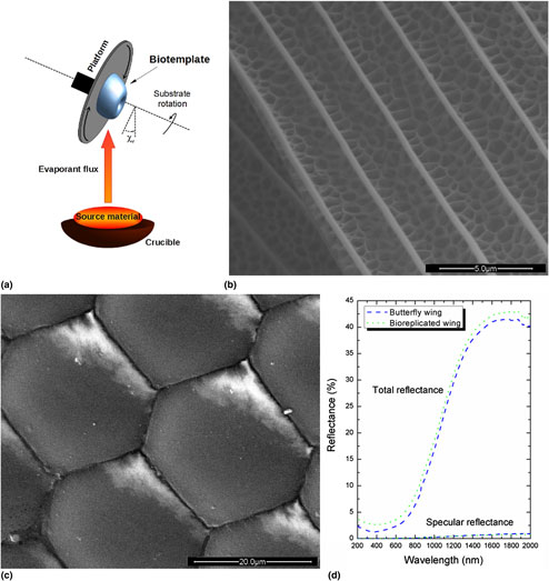
Bioreplication for optical applications
-
- Journal:
- MRS Communications / Volume 8 / Issue 2 / June 2018
- Published online by Cambridge University Press:
- 29 April 2018, pp. 220-225
- Print publication:
- June 2018
-
- Article
- Export citation
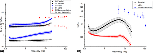
Oscillatory nanoindentation of highly compliant hydrogels: A critical comparative analysis with rheometry
-
- Journal:
- Journal of Materials Research / Volume 33 / Issue 8 / 27 April 2018
- Published online by Cambridge University Press:
- 27 April 2018, pp. 873-883
- Print publication:
- 27 April 2018
-
- Article
-
- You have access
- Open access
- HTML
- Export citation
