To save content items to your account,
please confirm that you agree to abide by our usage policies.
If this is the first time you use this feature, you will be asked to authorise Cambridge Core to connect with your account.
Find out more about saving content to .
To save content items to your Kindle, first ensure no-reply@cambridge.org
is added to your Approved Personal Document E-mail List under your Personal Document Settings
on the Manage Your Content and Devices page of your Amazon account. Then enter the ‘name’ part
of your Kindle email address below.
Find out more about saving to your Kindle.
Note you can select to save to either the @free.kindle.com or @kindle.com variations.
‘@free.kindle.com’ emails are free but can only be saved to your device when it is connected to wi-fi.
‘@kindle.com’ emails can be delivered even when you are not connected to wi-fi, but note that service fees apply.
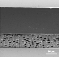
Electro-optical films composed of liquid crystal (LC) microdroplets encapsulated in an organically modified xerogel matrix were prepared by combined sol-gel and phase separation methods. The incorporation of a titanium alkoxide in the synthesis process as a co-precursor to silicon alkoxides was achieved without any destructive influence on the macroscopic LC phase separation. The consequent increase in the refractive index of the matrix satisfied the important criteria for high-performance films. The prepared films exhibit an outstanding 75.9% change in transmittance as an electric field is applied. An original setup was developed that enables the measurement of the film transmittance versus applied voltage at different temperatures over the full visible and near-infrared (near-IR) spectral range. For the first time, the relationship between these important characteristics (i.e., change in transmittance versus wave length versus temperature) was measured for a xerogel-dispersed LC composite film. The maximum of the curve increased and moved from the IR to the midvisible range with increasing temperature, achieving its maximum at 25.2 °C and 551 nm.
[Meza et al. J. Mater. Res.23(3), 725 (2008)] recently claimed that the correction factor beta for the Sneddon equation, used for the evaluation of nanoindentation load-displacement data, is strongly depth- and tip-shape-dependent. Meza et al. used finite element (FE) analysis to simulate the contact between conical or spheroconical indenters, and an elastic material. They calculated the beta factor by comparing the simulated contact stiffness with Sneddon’s prediction for conical indenters. Their analysis is misleading, and it is shown here that by applying the general Sneddon equation, taking into account the true contact area, an almost constant and depth-independent beta factor is obtained for conical, spherical and spheroconical indenter geometries.
Polypropylene–clay (Cloisite Na+) composites with clay contents in weight percentage (wt%) ranging from 1 to 15% were characterized for crystallization mechanism and kinetics. Combination of differential scanning calorimetry, transmission electron microscopy (TEM), and polarized light microscopy was used to investigate the crystallization behavior. Different crystallization mechanisms were observed in the matrix with 1–5 wt% nanoclay compared to the matrix with 10 and 15 wt% of nanoclay additive. TEM micrographs revealed intercalated and flocculated morphology for all the concentrates. At lower wt%, well-dispersed clay platelets acted as antinucleating agent and reduced polymer chain mobility. At high wt%, nucleation rate overcomes the slow diffusion rate. In the case of samples with higher wt% of nanoclay additives, segregation and precipitation of clay was observed in the interspherulite region. On the basis of crystallization kinetics and morphology results, a schematic model of the nanocomposite formation is proposed.
In view of the complexity of thin-film solar cells, which are comprised of a multitude of layers, interfaces, surfaces, elements, impurities, etc., it is crucial to characterize and understand the chemical and electronic structure of these components. Because of the high complexity of the Cu2ZnSn(S,Se)4 compound semiconductor absorber material alone, this is particularly true for kesterite-based devices. Hence, this paper reviews our recent progress in the characterization of Cu2ZnSnS4 (CZTS) thin films. It is demonstrated that a combination of different soft x-ray spectroscopies is an extraordinarily powerful method for illuminating the chemical and electronic material characteristics from many different perspectives, ultimately resulting in a comprehensive picture of these properties. The focus of the article will be on secondary impurity phases, electronic structure, native oxidation, and the CZTS surface composition.
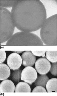
We describe the fabrication of core–shell colloidal spheres composed of a shell of tin sulfide and a core of polystyrene. The tin sulfide shell is deposited on micrometer-sized latex spheres using a sonochemical technique. By angle-dependent light scattering and electron microscopy, we find that the refractive index of the shell is 3.0 at a wave length of 1064 nm, and the shell’s thickness is controllable in the range of 30–60 nm. The resulting spheres have a narrow distribution of sizes, are stable in aqueous suspension, and are very strong scatterers in the near infrared with potential application in photonic band gap materials or other photonic devices.
The signification of the correction factor β that we defined for elastic material [J.M. Meza et al. J. Mater. Res.23(3), 725, (2008)] does not correspond to that of factor β in the Sneddon relationship between unloading contact stiffness, elastic modulus, and contact area as remarked by Durst et al. in their Comment (doi:10.1557/jmr.2012.41). To complete the results of Durst et al., the calculation of β is extended to a larger penetration depth range. It is shown that β depends on the depth to tip radius ratio, h/R, and on the Poisson’s ratio according to dimensionless analysis. The variation range of β is about 1.02–1.09 for 0.3 < h/R < 3 for purely elastic materials but can be much larger in case of elastic–plastic materials as shown [F. Abbes et al. J. Micromech. Microeng.20, 65003 (2010)].
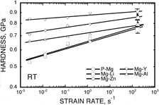
The effects of temperature and alloying elements on deformation in the high-strain-rate regime were investigated by testing fine-grained magnesium alloys with an average grain size of 2 ∼ 3 μm by a nanoindentation technique. The dynamic hardness measurements aligned well with existing quasistatic data, together spanning a wide range of strain rates, 10−3 ∼ 150/s. The high-rate hardness was influenced by various alloying elements (Al, Li, Y and Zn) to different degrees, consistent with expectations based on solid solution strengthening. Transmission electron microscopy observations of the indented region revealed no evidence for deformation twins for any alloying elements, despite the high strain-rate. The activation energy for deformation in the present alloys was found to be 85 ∼ 300 kJ/mol within the temperature range of 298 ∼ 373 K, corresponding to a dominant deformation mechanism of dislocation glide.
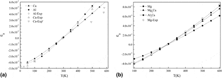
The use of Mg-Al-Ca alloys is limited mainly due to the hot crack defect. The exact mechanism of hot crack formation is not yet clearly understood. In this article, the hot crack mechanism is established from the present first-principles calculations based on the density functional theory and density functional perturbation theory . The thermal expansion behavior of Mg and the critical compounds Mg2Ca and Al2Ca in Mg-Al-Ca alloys is calculated. According to the present calculations, Mg2Ca is almost equal to Mg in thermal expansion, whereas the same in Al2Ca is much too lower. Al2Ca improves the creep resistance of Mg-Al-Ca alloys due to its high thermal stability, but it also accounts for the hot crack defect due to very small thermal expansion.
Asphalt bitumens are complex colloidal systems of high viscosity and complex behavior, which are mainly used for making asphalt concrete for road surfaces. Thermal and rheological characterizations are needed to understand their complex behavior, particularly at the processing stage. Prediction of properties at short and long observation times is usually performed through time-temperature superposition (TTS) models, which make use of some calculated shift factors. The influence of crystallization-like transformation processes on the validity of these shift factors is investigated here by temperature-modulated differential scanning calorimetry (TMDSC). Four asphalt emulsions are considered in this work, each one with a specific transformation behavior. The structure-properties relationships are explained on the basis of the transformation profiles and rheological data.
This paper reports on the defect structures formed upon strain relaxation in pulsed laser-deposited complex oxide superlattices consisting of the ferromagnetic metal, La0.67Sr0.33MnO3, and the antiferromagnetic insulator, La0.67Sr0.33FeO3. Atomic resolution scanning transmission electron microscopy and electron energy loss spectroscopy were used to characterize the structure and chemistry of the defects. For thinner superlattices, strain relaxation occurs through the formation of 2-D stacking faults, whereas for thicker superlattices, the prolonged thermal exposure during film growth leads to the formation of nanoflowers and cracks/pinholes to reduce the overall strain energy.
The high-density tungsten bronze (TB) Sr2-xCaxNaNb5O15 (SCNN, 0.05 ≤ x ≤ 030) lead-free ceramics were prepared by two-step solid-state reaction method. With increasing Ca2+ substitution, the crystal structure of SCNN ceramics slightly distorted from the TB tetragonal phase and became orthorhombic phase at room temperature. The smaller ionic radius of Ca2+ (1.34Å) compared with that of Sr2+ (1.44Å) contributed to the shrinkage of the crystal structure. Dielectric spectra of all compositions displayed two phase transitions: the ferroelastic orthorhombic to ferroelectric tetragonal phase transition (Te) at lower temperatures, and the ferroelectric to paraelectric phase transition (Tc) at higher temperatures. With increasing Ca2+ substitution, Te and Tc shifted towards higher temperature regions, while the maximum values of dielectric constant (εme and εm), Pr, Ec and d33 increased at first and then decreased. The ceramics with most homogeneous microstructure and highest density were obtained at x = 0.15, resulting in optimized properties.
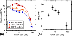
The hardening effect caused by the relaxation of nonequilibrium grain boundary structure has been explored in nanocrystalline Ni–W alloys. First, the kinetics of relaxation hardening are studied, showing that higher annealing temperatures result in faster, more pronounced strengthening. Based on the temperature dependence of relaxation strengthening kinetics, triple junction diffusion is suggested as a plausible kinetic rate limiter for the removal of excess grain boundary defects in these materials. Second, the magnitude of relaxation strengthening is explored over a wide range of grain sizes spanning the Hall–Petch breakdown, with an apparent maximum hardening effect found at a grain size below 10 nm. The apparent activation volume for plastic deformation is unaffected by annealing for grain sizes down to ∼10 nm, but increases with annealing for the finest grain sizes, suggesting a change in the dominant deformation mechanism for these structures.
In this work, we find that the pressure-induced phase transition of InP from III-V semiconductor phase having zincblende (ZB) crystal structure to metallic phase having rocksalt (RS) structure occurs at a pressure of 8.56 GPa accompanied by an 18% volume collapse. It is found that the nearest In and P atoms bonded as covalent bond. Crystal space of ZB is just occupied by In-P tetrahedrons partly with many interstices, but that of RS is fulfilled by close-packed octahedrons entirely. With pressures, broadened energy band of antibonding state and the reduced density of states (DOS) of bonding state cause the weakening of tetrahedral In-P covalent bonds. And then, ZB is destroyed and rebuilt to RS structure. Some In-5s, In-5p, P-3p and a few P-3s move to unoccupied high energy level, across Fermi level, and migrate from valence band to conduction band, and then generate metallic properties. Furthermore, changes of covalent bond would cause evident variation of elastic properties on the {100} and {110} planes.
In this article, single-phase CuIn(SxSe1-x)2 thin films with different x have been prepared using a new two-step method consisting of partly selenizing Cu–In precursors in Se ambient, and then exposing the partly selenized films to H2S/Ar under different conditions. The x-ray diffraction indicated that the CuIn(SxSe1-x)2 films exhibited the homogeneous chalcopyrite structure. With the increase of the sulfurization temperature from 425 to 525 °C, x increases from 0 to 1, Eg increases from 0.95 to 1.42 eV, the Raman shift of the A1[Se–Se] mode increases from 173 to 197 cm−1, and the resistivity increases from 101 to 103 Ω.cm.
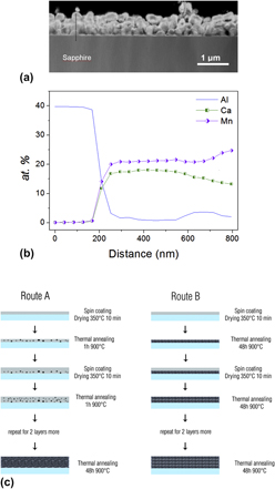
Polycrystalline randomly oriented CaMnO3 films were successfully deposited on sapphire substrates by soft chemistry methods. The precursor solutions were obtained from a mixture of metal acetates dissolved in acids. The Seebeck coefficient and the electrical resistivity were measured in the temperature range of 300 K < T < 1000 K. Modifications of thermal annealing procedures during the deposition of precursor layers resulted in different power factor values. Thermal annealing of CaMnO3 films at 900 °C for 48 h after four-layer depositions (route A) resulted in a pure perovskite phase with higher power factor and electrical resistivity than four-layer depositions of films annealed layer by layer at 900 °C for 48 h (route B). The studied films have negative Seebeck coefficients indicative of n-type conduction and electrical resistivities showing semiconducting behavior.
Reflow behavior of a Sn–8.5Zn–0.5Ag–0.01Al–0.1Ga (five-element) solder on the Ni/Cu substrate was investigated under different heating rates. Reflowed samples show decreased Zn and increased AgZn3 in the solder with a reduction in the heating rate. The Zn at the solder/substrate interface was found to be much lower than that in the Sn–Zn solder systems. Cu was observed to be diffused through the electroplated Ni layer and noticed only with the Ag–Zn compound in the solder. Ga was spotted at the interface in the Ag–Zn matrix, whereas Al was detected with the Zn at the interface. Small intermetallic compound (IMC) layer was formed at the interface; however, its amount enhanced with the reduction in the heating rate. Present study relates the reflow behavior of the five-element solder with the reactivity of different elements in the system and its influence on the formation of IMCs in the solder and at the solder/substrate interface.
The aim of this study was the development of biocomposite scaffolds (membranes and matrices) based on natural polymers used for bone tissue engineering. The novelty featured in this paper is the use of phosphorylated dextran (PDex) as natural component in collagen-based biocomposites. The PDex both in acid form and as mixed salts of Mg–Na, Zn–Na, Ca-Na was characterized by Fourier transform infrared spectroscopy (FTIR), nuclear magnetic resonance (NMR) spectroscopy, potentiometric and conductometric titration and energy dispersive x-ray spectroscopy (EDX) analysis. The biocomposite scaffolds were obtained by freeze-drying as matrices and by free-drying as membranes with specific microporous morphological structures that depended on drying process of collagen gels with PDex. The biocomposites were physical–chemical characterized by differential scanning calorimetry (DSC) and, water and water vapor absorption. The biocompatibility was evaluated in vitro with human osteosarcoma MG 63 cell lines. The results showed that biocompatibility was improved by the use of PDex as mixed salts of Mg–Na, Zn–Na, Ca-Na in collagen biocomposites.
A nanoparticle catalyst of PtRuAu/C was synthesized by including an Au precursor in the radiolytic process for preparing a PtRu/C catalyst. Their methanol oxidation activity and electrochemical durability were measured by linear sweep voltammetry before and after potential cycling treatment. PtRuAu/C had a significantly higher durability than PtRu/C while maintaining a comparable high activity. The morphology and substructure of the nanoparticles were investigated by energy-dispersive x-ray spectroscopy, x-ray diffraction, and x-ray absorption fine structure spectroscopy. Metallic nanoparticles with diameters of about 2 nm were obtained; they probably had Pt-core/PtRu-shell structures. Transmission electron microscopy observations after potential cycling revealed that 2-nm-diameter nanoparticles containing Au did not coarsen, whereas nanoparticles without Au coarsened significantly to 3.7 nm. Some crystal defaults were observed in the coarsened particles, implying that the coarsening was caused by Ostwald ripening. The Au addition to catalyst particles consisting of PtRu inhibits coarsening and consequently improves the electrochemical durability.
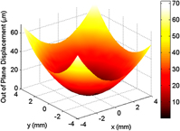
Characterizing the residual stress of thick nanocrystalline electrodeposits poses several unique challenges due to their fine grain structure, thickness distribution, and matte surface. We use a three-dimensional profilometry-based approach that addresses each of these complicating factors and enables quantitative analysis of residual stress with reasonable accuracy. The specific emphasis of this work is on thick (10–100 μm), nanocrystalline Ni-W electrodeposits of the finest grain sizes (4–63 nm), in which residual stresses arise during the deposition process as well as during postdeposition annealing. The present measurements offer quantitative insight into the mechanisms of stress development and evolution in these alloys, suggesting that the grain boundary structure is out of equilibrium (unrelaxed) and contains the excess free volume that controls the resulting residual stress levels in these films. There are apparently two factors contributing to this stress: the percentage of excess free volume contained in the grain boundaries, which is affected by the processing conditions, and the total volume fraction of grain boundaries, which is controlled by the grain size.
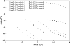
A single crystal aluminum nitride (AlN) wafer surface was investigated via the use of a novel software-based, Charge-based Deep Level Transient Spectroscopy (Q-DLTS) apparatus, both before and after surface bond termination with hydrogen plasma. The sample was cleaned and metalized with a thermoresistive evaporator to create electrical contacts and then annealed in a helium atmosphere at 825 °C. Current-voltage (I-V) measurements were performed to investigate the nature of the metal/substrate contacts. The effect of hydrogen termination was investigated and Arrhenius plots were produced from Q-DLTS spectra at temperatures ranging from −15.9 °C to 136.0 °C. Activation energies and capture cross-section values were calculated from the Q-DLTS spectra for traps existing in the AlN substrate surface. Prior to hydrogen termination, four charge traps were observed with activation energies of 0.31 eV, 0.61 eV, 0.56 eV, and 0.18 eV and capture cross sections 5.6 × 10⁻²¹ cm2, 1.1 × 10⁻¹⁶ cm2, 3.5 × 10⁻¹⁹ cm2, and 1.3 × 10⁻²¹ cm2, respectively After hydrogen termination, five charge traps were observed with activation energies of 0.31 eV, 0.61 eV, 0.52 eV, 0.19 eV, and 0.40 eV, and capture cross sections 4.9 × 10⁻²¹ cm2, 1.3 × 10⁻¹⁶ cm2, 2.9 × 10⁻¹⁹ cm2, 3.1 × 10⁻¹⁹ cm2, and 4.7 × 10⁻¹⁹ cm2, respectively. Four of these peaks after termination are matched with the peaks prior to termination and the fifth peak appears to be the result of the hydrogen termination.