To save content items to your account,
please confirm that you agree to abide by our usage policies.
If this is the first time you use this feature, you will be asked to authorise Cambridge Core to connect with your account.
Find out more about saving content to .
To save content items to your Kindle, first ensure no-reply@cambridge.org
is added to your Approved Personal Document E-mail List under your Personal Document Settings
on the Manage Your Content and Devices page of your Amazon account. Then enter the ‘name’ part
of your Kindle email address below.
Find out more about saving to your Kindle.
Note you can select to save to either the @free.kindle.com or @kindle.com variations.
‘@free.kindle.com’ emails are free but can only be saved to your device when it is connected to wi-fi.
‘@kindle.com’ emails can be delivered even when you are not connected to wi-fi, but note that service fees apply.
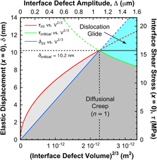
Under electrochemical cycling, stress intensification and relaxation within small volumes at the lithium/solid-state electrolyte (SSE) interface are thought to be critical factors contributing to mechanical failure of the SSE and subsequent short-circuiting of the device. Nanoindentation has been used to examine the diffusion-limited pressure lithium can support in the absence of active dislocation sources at high homologous temperatures. Based on the underlying physics of this deformation mechanism, a simple perturbation model coupling local current density, elastic stress, and diffusional creep relaxation is introduced. Combining this analysis with the indentation results, it is possible to describe a defect length scale which is too large for effective diffusional creep relaxation, but too small for efficient dislocation multiplication. In this instance, the properties of the SSE may become critical, and relevant indentation results of the SSE are described. The final outcome of the proposed analysis is a newly developed deformation mechanism map.
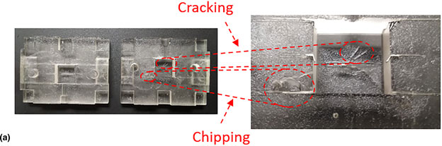
This Prospective covers an overview of the injection molding process and the importance of mold design and tooling considerations, important material requirements and thermal properties for molds, polymer material requirements for injection molding, mold flow analysis, and the promise of using the 3D printing process for mold fabrication. The second part demonstrates the injection molding process using 3D-printed polymer molds and its suitability for low-run productions. 3D-printed molds using stereolithography and fused filament fabrication have been injected with polylactic acid, and the quality of the injected parts was assessed in terms of dimensional accuracy and the damage mechanisms during fabrication.
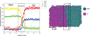
The molybdenum disulfide (MoS2) and indium tin oxide (ITO) interface were studied by atom probe tomography (APT). Raman spectroscopy, scanning electron microscopy, and grazing-incidence x-ray diffraction measurements were performed as complementary characterization. Results confirm that nanowires plated shape with the 〈110〉-orientation are aligned perpendicular to the ITO film with principal reflections at (002), (100), (101), (201), and Raman spectroscopy vibrational modes at E12g at 378 cm−1 and A1g at 407 cm−1 correspond to 2H-MoS2. APT reveals MoS+2, MoS+3 as predominant evaporated molecular ions on the sample, indicating no significant diffusion/segregation of Mo or S species within the ITO layer.
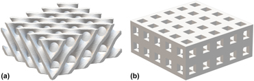
Scaffolds based on two different geometries were constructed by additive manufacturing: one based on a triply periodic minimal surface, the Schwarz D surface, and the other based on a rectangular geometry with orthogonal through-holes. For construction of the scaffolds, two different materials were used: polylactic acid (PLA) in filament form and alumina in printable paste form. The structure of the resulting scaffolds was characterized via X-ray diffraction and scanning electron microscopy, and cell proliferation was assessed for each geometry and material, using fluorescence microscopy and DNA quantification via NanoDrop. Additive manufacturing allowed us to obtain scaffolds with the assessed materials while guaranteeing the interconnectivity of the pores in each one. The curved surfaces constructed with PLA were more favorable for cell attachment and proliferation of the CHO-K1 cell line.
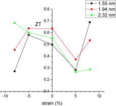
In this article, the strain-dependent thermoelectric performance of circular porous armchair silicene nanoribbons (ASiNRs) under uniaxial tension and compression is computed by means of a semiempirical approach in combination with nonequilibrium Green’s function. Our findings clearly demonstrate that the thermoelectric performance can be effectively tuned by the optimum choice of the nature and magnitude of the strain depending on the pore size. For smaller pore sizes, higher tensile strains can be preferred whereas for nanostructures with larger pores, the compression is a suitable option. Further analysis concludes that the tensile deformation fails to attain any improvement in the thermoelectric figure of merit ZT at any choice of temperature, whereas the performance under compressive deformation goes on improving with the increase in the applied temperature. In addition, changing the pore shape to a triangular one is found to significantly enhance the thermoelectric performance.
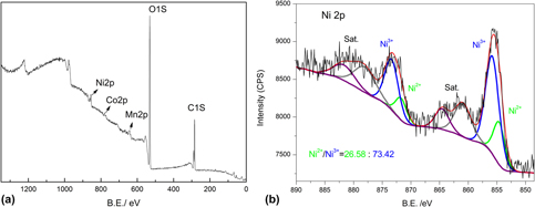
Nickel-rich layered oxide LiNi0.8Co0.1Mn0.1O2 suffers from severe structural instability and irreversible capacity loss during cycling due to cation disorder of Li+ and Ni2+. To solve this problem, the precursor Ni0.8Co0.1Mn0.1(OH)2 and well-ordered LiNi0.8Co0.1Mn0.1O2 cathode materials were successfully synthesized via controlled crystallization and high-temperature solid-state methods. The structure, morphology, and electrochemical performance of the precursor and LiNi0.8Co0.1Mn0.1O2 powders were investigated. The results show that the precursor Ni0.8Co0.1Mn0.1(OH)2 is made of sphere-like particles composed of needle-like primary crystal and LiNi0.8Co0.1Mn0.1O2 possesses a perfect layered structure with low Li/Ni disorder. Electrochemical data demonstrate that the material rate capabilities are 203.3, 187.7, 170.4, and 163 mA h/g from 0.1C to 10C, respectively. The capacity retention is 87.9% after 100 cycles at 1C, even the cut-off voltage was increased to 4.5 V. The high discharge capacity and outstanding cycling life can be attributed to the merits of a perfect crystal lattice with low Li/Ni disorder, fast lithium ion transport, and relatively low charge transfer resistance.
Silver/titanium dioxide (Ag/TiO2) membranes were successfully deposited on poly(sulfone amide) substrates by direct current magnetron sputtering and radio frequency magnetron sputtering techniques with pure silver (Ag) and TiO2 targets. The prepared membranes were systematically characterized by scanning electron microscopy X-ray diffraction, insulation tests, and Fourier transform infrared spectrometry. The dependence of the main sputtering parameters on optical and thermal properties of the film was investigated by an orthogonal analysis method. Optimal parameters of fabricate Ag/TiO2 membranes with better comprehensive performances could be obtained ultimately. The infrared reflection rate and temperature difference of the Ag/TiO2 film deposited with the optimized parameters were 81.6% and 90 °C, respectively. The high infrared reflection and excellent thermal conductivity properties of the Ag/TiO2 composite membrane make it a promising candidate for thermal insulating coatings on fabrics, and can be used for the development of high-performance protective garments in the future.
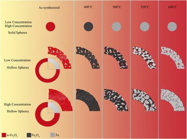
The global market requirement of ultra-fine iron powder (UFIP), with a range size of 0.1–1 μm, is more than 20,000 tons per annum. However, no low-cost nontoxic synthesis route of UFIP is known. In this study, we used the low-cost, rapid, and scalable flame aerosol synthesis (FAS) method to synthesize iron oxide nanoparticles with different size and morphology. Combining with a postreduction heat treatment process, a feasible synthesis route of UFIP which meets the commercial production criteria has been developed. By optimizing the precursor concentration and postreduction heat treatment parameters, the final particle size of UFIP can be controlled. The evolution of the microstructure, phase formation, and magnetic properties during the postreduction heat treatment are systematically investigated, and a feasible reaction model has been established. This work provides an important starting point for the facile commercial synthesis of UFIP and can be readily expanded to other pure metals.
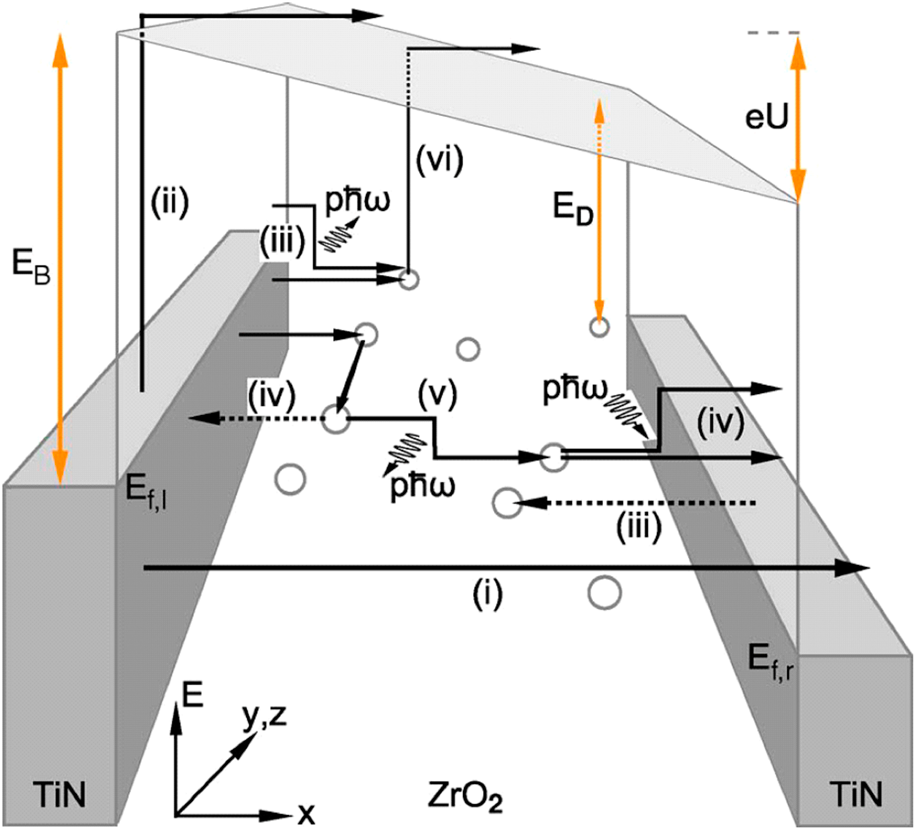
Capacitors represent the largest obstacle to dynamic random-access memory (DRAM) technology evolution because the capacitor properties govern the overall operational characteristics of DRAM devices. Moreover, only the atomic layer deposition (ALD) technique is used for the dielectric and electrode because of its extreme geometry. Various high-k materials deposited by ALD have been investigated for further scaling. Whereas past investigations focused on increasing the physical thickness of the dielectric to suppress leakage current, the physical thickness of the dielectric should also be limited to a few nanometers in design rules less than 1×-nm. Therefore, a new way to overcome the limitations of traditional approaches based on thorough understanding of high-k materials is highly recommended to enhance the properties of conventional materials and provide directions for developing new materials. In this review, previously reported results are discussed, and suggestions are made for further investigations for DRAM capacitor applications.
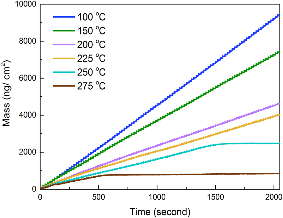
In this work, we studied an atomic layer deposition (ALD) process of ZrO2 with the precursors of tetrakis(dimethylamido)zirconium(IV) and water. We investigated the growth characteristics and mechanism of the ALD ZrO2 in the temperature range of 50–275 °C. Furthermore, the evolutions of film thickness and morphology were studied and discussed. It was found that the growth rate of ZrO2 decreased almost linearly with the increasing temperature from ∼1.81 Å/cycle at 50 °C to ∼0.8 Å/cycle at 225 °C. Interestingly, it was revealed that the growth of ZrO2 films ceased after a certain number of ALD cycles at a temperature higher than 250 °C. We also verified that the crystallinity of ZrO2 evolved with deposition temperature from amorphous to crystalline phase. In addition, the wettability of ZrO2 films was studied, showing a hydrophobic nature.
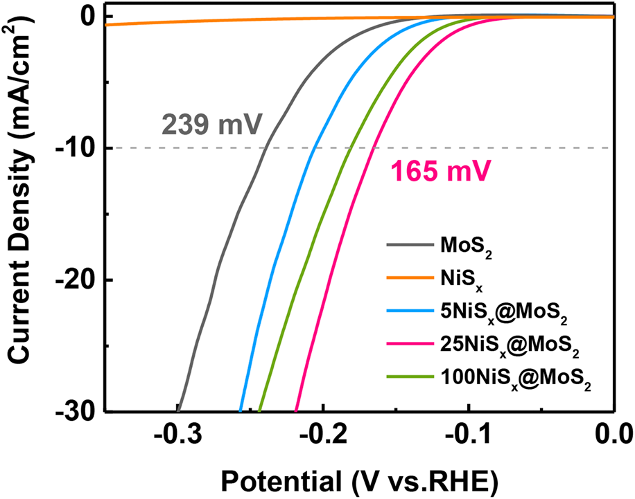
Developing low-cost and high-performance hydrogen evolution reaction (HER) electrocatalysts is essential for the development of hydrogen energy. While transition metal sulfides are reported as promising HER electrocatalysts, their performance still requires further improvement for practical application. In this work, we report a strategy to construct NiSx@MoS2 heterostructures with a well-defined interface structure by growing NiSx nanoclusters on MoS2 nanosheets through atomic layer deposition (ALD). NiSx@MoS2 heterostructures exhibit strongly enhanced HER activity with lower overpotential and faster reaction dynamic compared to MoS2 and NiSx single phases. The enhanced performance is attributed to improved adsorption of the reaction intermediates and the facilitated charge transfer process near the MoS2/NiSx interfaces. Besides high activity, NiSx@MoS2 heterostructures also exhibit high stability in alkaline media. The methodology and knowledge in this work can guide the rational design of high-performance electrocatalysts through hetero-interface engineering.
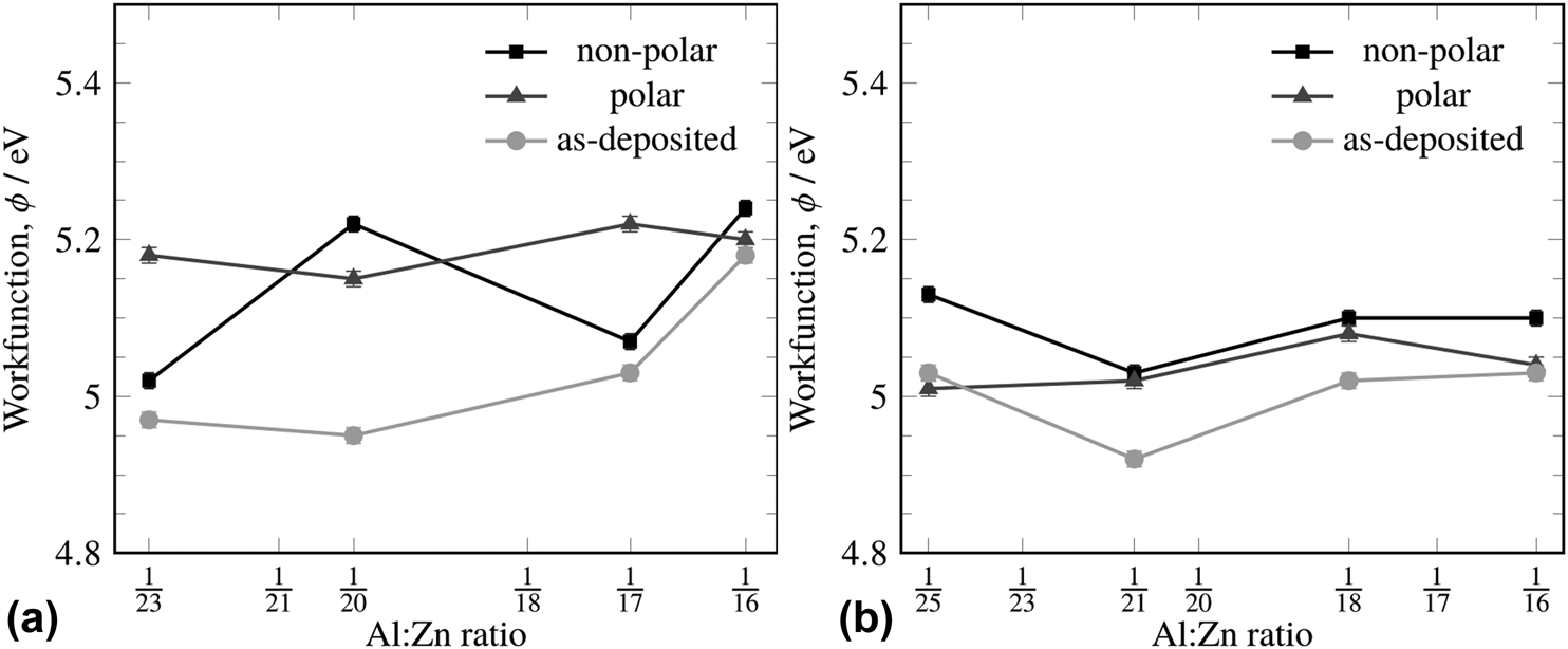
Al-doped ZnO (AZO) is a promising earth-abundant alternative to Sn-doped In2O3 (ITO) as an n-type transparent conductor for electronic and photovoltaic devices. We have deposited AZO films with resistivities as low as 1.1 × 10⁻³ Ω·cm by atomic layer deposition (ALD) using trimethylaluminum (TMA), diethylzinc (DEZ), and water at 200 °C. The work functions of the films were measured using a scanning Kelvin probe (sKP) to investigate the role of aluminum concentration. The work function of AZO films prepared by two different ALD recipes were compared: a “Al-terminated” recipe and a “ZnO-terminated” recipe. As aluminum doping increases, the Al-terminated recipe produces films with a consistently higher work function than the ZnO-terminated recipe. The resistivity of the Al-terminated recipe films shows a minimum at a 1:16 Al:Zn atomic ratio and using a ZnO-terminated recipe, minimum resistivity was seen at 1:19. The film thicknesses were characterized by ellipsometry, chemical composition by EDX, and resistivity by a four-point probe.
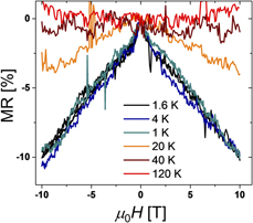
The authors summarize the results of selective-area growth of vertical MnAs/InAs heterojunction nanowire (NW) arrays and present a preliminary characterization of the transport properties of a single MnAs/InAs heterojunction NW and a single InAs host NW for MnAs inclusions. During the endotaxy of MnAs after the selective-area growth of host InAs nanowires (NWs) on partially SiO2-masked GaAs(111)B substrates, hexagonal NiAs-type MnAs nanoclusters (NCs), which exhibit spontaneous magnetization at room temperature, are formed with the 〈0001〉 direction oriented parallel to the 〈111〉B direction of the zinc-blende-type InAs host NWs. For InAs host NWs, a large positive ordinary magnetoresistance (MR) effect up to 165% is observed at temperatures between 7 and 280 K. In addition, magnetotransport measurements reveal universal conductance fluctuations and a weak Anderson localization at temperatures up to 20 K due to a charge-accumulation layer formed at the surface. Single MnAs/InAs heterojunction NWs, however, exhibit only a negative MR effect, which is independent of temperature T < 10 K and linearly decreases up to −10% at 10 T with increasing magnetic field. These results reveal the tremendous influence of ferromagnetic NCs on the transport behavior inside the InAs host NWs.
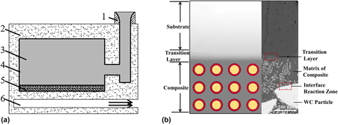
In this study, cast tungsten carbide particle/steel matrix surface composites were fabricated using a vacuum evaporative pattern casting (V-EPC) infiltration process. Through thermal shock tests at 500 °C, the initiation and propagation of cracks at the interface of the composites were investigated. Owing to the mismatch in the coefficients of thermal expansion (CTE), cracks tended to appear at the interface reaction zone (IRZ) between the particles and the matrix. Because there was also a difference in the CTE between the composite and the substrate, the cracks propagated rapidly along the transition layer (TL) between the composite and the substrate, and finally connected to form macro-cracks. Based on the stress analysis and calculation, the maximum thermal stress at the TL was 63.4 MPa, while the maximum thermal stress at the IRZ was 38 MPa. It could thus be inferred that the TL is the weak link under thermal fatigue. In addition, the experimental results were verified and found to be in good agreement with the calculations.
Iron carbide (Fe1−xCx) thin films were successfully grown by plasma-enhanced atomic layer deposition (PEALD) using bis(N,N′-di-tert-butylacetamidinato)iron(II) as a precursor and H2 plasma as a reactant. Smooth and pure Fe1−xCx thin films were obtained by the PEALD process in a layer-by-layer film growth fashion, and the x in the nominal formula of Fe1−xCx is approximately 0.26. For the wide PEALD temperature window from 80 to 210 °C, a saturated film growth rate of 0.04 nm/cycle was achieved. X-ray diffraction and transition electron microscope measurements show that the films grown at deposition temperature 80–170 °C are amorphous; however, at 210 °C, the crystal structure of Fe7C3 is formed. The conformality and resistivity of the deposited films have also been studied. At last, the PEALD Fe1−xCx on carbon cloth shows excellent electrocatalytic performance for hydrogen evolution.
Nanostructures are considered to have great potential and are widely used in energy storage and sensing devices, and atomic layer deposition (ALD) is of great help for better nanostructure fabrications. ALD can help to preserve the original properties of materials, and, meanwhile, the excellent film quality, nanoscale precise thickness control, and high conformality also play important role in fabrication process. To enhance the performance of energy storage and sensor devices, ALD has been used in directly fabricating active nanostructures, depositing protective passivation layers, etc. ALD is a convenient technique which has been widely engaged in energy-related fields including electrochemical conversion and storage, as well as in sensor and biosensors. The related research interest is increasing significantly. In this review, we summarize some of the latest works on ALD for batteries, supercapacitors, and sensors, and demonstrate the benefits of ALD comprehensively. In these devices, different materials are deposited by ALD under different conditions to achieve better battery performance, higher supercapacitor capacitance, and higher sensitivity. This review fully presents the strengths of ALD and its application in energy storage and sensing devices and proposes the future prospects for this rapidly developing technology.